
Compositions and methods for controlled polishing of copper

a technology of mechanical planarization and control, applied in lapping machines, other chemical processes, manufacturing tools, etc., can solve problems such as affecting the continued fabrication of dual damascene structures, unwanted interconnection metals, and electrical signals

Inactive Publication Date: 2005-06-23
ROHM & HAAS ELECTRONICS MATERIALS CMP HLDG INC
View PDF16 Cites 42 Cited by
  • Summary
  • Abstract
  • Description
  • Claims
  • Application Information

AI Technical Summary

Benefits of technology

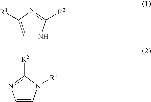
[0009] In a third aspect, the present invention provides a method for polishing copper from a semiconductor wafer comprising: contacting the wafer with a polishing composition, the wafer containing the copper, the polishing composition comprising by weight percent 0.001 to 6 inhibitor for a nonferrous metal, 0.05 to 10 complexing agent for the metal, 0.01 to 25 imidazole, 0.5 to 40 abrasive, 0 to 10 oxidizer, 0 to 10 selected from the group comprising, polyvinylpyrrolidone, polyvinyl alcohol and mixtures thereof and balance water; and polishing the wafer with a polishing pad, wherein the imidazole accelerates the polishing of the copper.

Problems solved by technology

Unfortunately, CMP processes often result in unwanted interconnect metals from inadequate second step polishing.
This unwanted metal can compromise electrical signals and impair continued fabrication of dual damascene structures.
Unfortunately, such known compositions may create unwanted copper, a condition known as “proud copper”.

Method used


Image

  • Compositions and methods for controlled polishing of copper
  • Compositions and methods for controlled polishing of copper
  • Compositions and methods for controlled polishing of copper

Examples


example 1

[0042] This experiment measured removal rates of the tantalum nitride barrier, a dielectric layer of carbon doped oxide and copper from a semiconductor wafer. In particular, the test determined the effect of the addition of imidazole to the removal rates of copper in a second step polishing operation, as a function of the concentration of the BTA. A Strausbaugh polishing machine using a Politex polyurethane polishing pad (Rodel, Inc.) under downforce conditions of about 1.5 psi and a polishing solution flow rate of 200 cc / min, a platen speed of 93 RPM and a carrier speed of 87 RPM planarized the samples. The polishing solutions had a pH of 9 adjusted with KOH and HNO3. All solutions contained deionized water. In addition, polishing solutions included 12 weight percent silica abrasives having an average particle size of 50 nm.

TABLE 1Second Step Polishing ResultsImidazoleBTACuCDOTaNRatioTest(wt %)(wt %)(Å / min)(Å / min)(Å / min)Imidazole / BTAA—0.05192205884—10.100.02199196893520.500.02495...

example 2

[0044] In this experiment, the static etch rate of the copper with the addition of imidazole was measured with a static electrochemical cell. All example solutions were the same as Example 1 above. The slurry static etch rate (Å / min) was determined from the calculated average Ecorr / Icorr values of the test samples.

TABLE 2ImidazoleAvg. EcorrAvg IcorrStatic EtchTest(wt %)(mV)(uA / Cm2)(Å / min)A02311.630.3610.12401.870.4120.82502.810.62

[0045] As illustrated in Table 2 above, as the concentration of the imidazole increased, there was an increase in the copper static etch rate. In particular, the static etch rate was increase to 0.62 Å / min from 0.36 Å / min when 0.8 weight percent of the imidazole was added to the Test sample A which contained 0 weight percent imidazole. Additionally, the static etch rate was within acceptable rates to avoid corrosion problems.


PUM

PropertyMeasurementUnit
weight percentaaaaaaaaaa

Abstract

The present invention provides an aqueous composition useful for polishing copper on a semiconductor wafer comprising by weight percent 0.001 to 6 inhibitor for a nonferrous metal, 0.05 to 10 complexing agent for the metal, 0.01 to 25 copper removal agent for accelerating the removal of the copper, 0.5 to 40 abrasive, 0 to 10 selected from the group comprising, polyvinylpyrrolidone, thermoplastic polymer and mixtures thereof, wherein the copper removal agent is imidazole.

Description

BACKGROUND OF THE INVENTION [0001] The invention relates to chemical mechanical planarization (CMP) of semiconductor wafer materials and, more particularly, to CMP compositions and methods for removing interconnect metals from semiconductor wafers in the presence of dielectrics and barrier materials. [0002] Typically, a semiconductor wafer has a wafer of silicon and a dielectric layer containing multiple trenches arranged to form a pattern for circuit interconnects within the dielectric layer. The pattern arrangements usually have a damascene structure or dual damascene structure. A barrier layer covers the patterned dielectric layer and a metal layer covers the barrier layer. The metal layer has at least sufficient thickness to fill the patterned trenches with metal to form circuit interconnects. [0003] CMP processes often include multiple planarization steps. For example, a first step removes a metal layer from underlying barrier dielectric layers. The first step polishing removes...

Claims


Application Information

Patent Timeline
Patent Type & Authority Applications(United States)
IPC IPC(8): B24B37/00B24D3/02C09G1/02C09K3/14H01L21/302H01L21/304H01L21/321H01L21/461
CPCH01L21/3212C09G1/02C09K3/1463C09K3/14
Inventor AMEEN, JOSEPH G.LAVOIE, RAYMOND LEE JR.QUANCI, JOHNSO, JOSEPH K.THOMAS, TERENCE M.YE, QIANQIU
Owner ROHM & HAAS ELECTRONICS MATERIALS CMP HLDG INC
Learn More