System and method for on-board timing margin testing of memory modules

a technology of memory modules and timing margins, which is applied in the field of processor-based systems, can solve the problems of slow memory controllers and memory devices, limiting the data bandwidth between the processor and the memory device, and increasing the operating speed of processors, and achieves the effect of high operating speed

Inactive Publication Date: 2005-03-17
ROUND ROCK RES LLC
View PDF99 Cites 67 Cited by
  • Summary
  • Abstract
  • Description
  • Claims
  • Application Information

AI Technical Summary

Benefits of technology

[0013] A memory module for a processor-based system includes a plurality of memory devices coupled to a memory hub. The memory hub includes a link interface for receiving memory requests for access to the memory devices and at least one memory device interface coupled to the memory devices. The memory device interface couples write memory requests and write data to the memory devices, and couples read memory requests to the memory device and read data from the memory device. The memory hub also includes a self-test module coupled to the memory devices. The self-test module is operable to couple to the memory devices a series of corresponding first and second signals. Significantly, the self-test module alters the relative

Problems solved by technology

Although the operating speed of memory devices has continuously increased, this increase in operating speed has not kept pace with increases in the operating speed of processors.
The relatively slow speed of memory controllers and memory devices limits the data bandwidth between the processor and the memory devices.
In addition to the limited bandwidth between processors and memory devices, the performance of computer systems is also limited by latency problems that increase the time required to read data from system memory devices.
Therefore, although SDRAM devices can synchronously output burst data at a high data rate, the delay in initially providing the data can significantly slow the operating speed of a computer system using such SDRAM devices.
Although there are advantages to utilizing a memory hub for accessing memory devices, the design of the hub memory system, and more generally, computer systems including such a memory hub architecture, becomes increasingly difficult.
However, as transfer rates increase, the time for which a signal represents valid information is decreasing.
In the case of timing skew of signals, it often arises from a variety of timing errors such as loading on the lines of the bus and the physical lengths of such lines.
As data eyes of the signals decrease at higher transfer rates, it is possible that one or more of a group of signals provided in parallel will have arrival times such that not all signals are simultaneously valid at a receiving entity, and thus cannot be successfully captured that entity.
In this situation, the signals having non-overlapping data eyes are not valid at the same time as the rest of the signals, and consequently, cannot be successfully captured by the receiving entity.
Clearly, as those ordinarily skilled in the art will recognize, the previously described situation is unacceptable.
As it is further recognized by those familiar in the art of high speed digital systems, signal timing is an issue that has become increasingly more significant in the design of systems capable of transferring and transmitting information at high speeds because signal timing can be affected by many things.
However, such probes can introduce loading effects that change the characteristic of the signals being evaluated.
Although probes are specifically designed to have high impedance and low capacitance to minimize loading issues and the introduction of noise, there is still in many cases, an unacceptable level of loading that changes the character of a signal to such a degree that it cannot be accurately evaluated.
Also, the propagation delays in coupling signals between the integrated circuit nodes and the test equipment may introduce delays that make it impossible to accurately determine timing relationships within the integrated circuit.
However, there can be no assurance that the command and address signals and the write data signals are actually coupled to circuit nodes in the memory device with this same range of timing relationships.
Therefore, the memory device may not actually function properly with the timing relationships that were used during the testing.
The difficulty in accurately controlling and / or determining the actual timing relationships between signals applied to or internal to memory devices is exacerbated when the memory devices are accessible only through interface circuitry.
Although production testing equipment may be able to accurately control and determine the timing relationships between signals applied to the interface circuitry, such equipment cannot control or determine the timing relationships of the signals in the memory devices after the devices have been packaged with the interface circuitry so that the signals coupled to and from the memory devices must be coupled through the interface circuitry.
Another problem that can be encountered in testing high-speed memory devices using conventional production testing equipment is associated with obtaining control over the memory bus in order to perform evaluation.
Again, this problem is exacerbated when memory devices are accessible to production testing equipment only through interface circuitry, such as a memory hub.
Unless control over the memory bus can be obtained, analysis becomes a difficult task.
However, obtaining control over the memory bus is a difficult task in itself because conventional approaches often interfere with the normal operation of the computer system, thus, preventing accurate analysis of the memory system under true, normal operating conditions.

Method used


Image

  • System and method for on-board timing margin testing of memory modules
  • System and method for on-board timing margin testing of memory modules
  • System and method for on-board timing margin testing of memory modules

Examples


Embodiment Construction

[0017] Embodiments of the present invention are directed to a memory hub module having the capability to self-test signal timing relationships. Certain details are set forth below to provide a sufficient understanding of various embodiments of the invention. However, it will be clear to one skilled in the art that the invention may be practiced without these particular details. In other instances, well-known circuits, control signals, and timing protocols have not been shown in detail in order to avoid unnecessarily obscuring the invention.

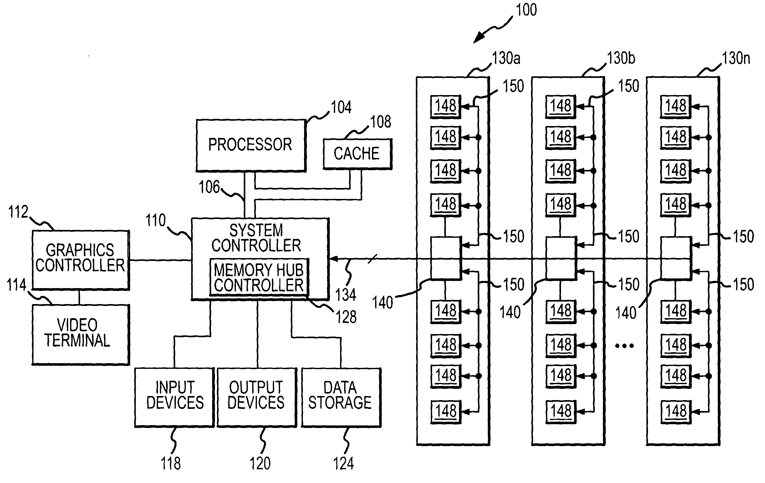
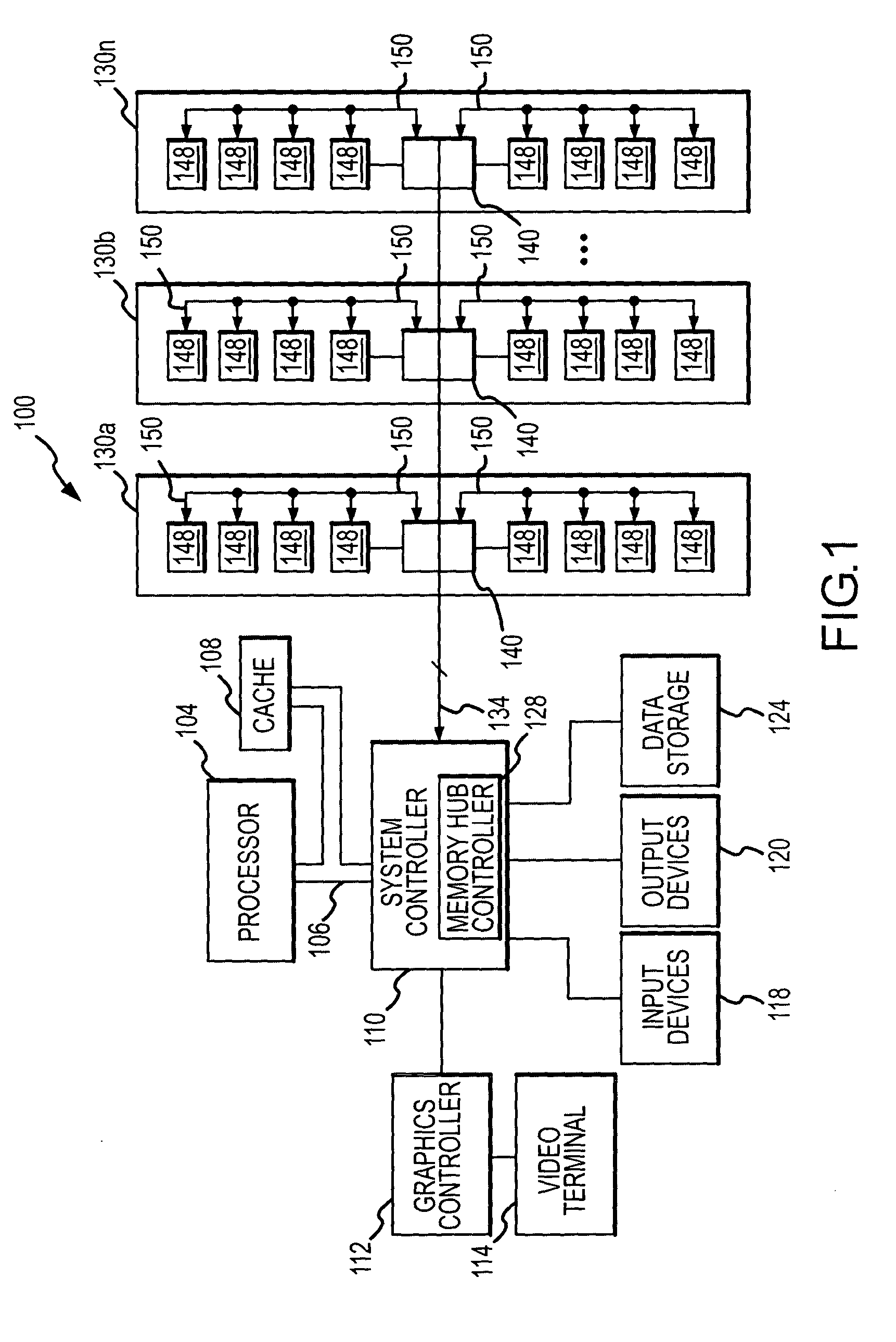
[0018] A computer system 100 according to one embodiment of the invention is shown in FIG. 1. The computer system 100 includes a processor 104 for performing various computing functions, such as executing specific software to perform specific calculations or tasks. The processor 104 includes a processor bus 106 that normally includes an address bus, a control bus, and a data bus. The processor bus 106 is typically coupled to cache memory 108, whi...


PUM


Abstract

A memory module includes several memory devices coupled to a memory hub. The memory hub includes several link interfaces coupled to respective processors, several memory controller coupled to respective memory devices, a cross-bar switch coupling any of the link interfaces to any of the memory controllers, a write buffer and read cache for each memory device and a self-test module. The self-test module includes a pattern generator producing write data having a predetermined pattern, and a flip-flop having a data input receiving the write data. A clock input of the flip-flop receives an internal clock signal from a delay line that receives a variable frequency clock generator. Read data are coupled from the memory devices and their pattern compared to the write data pattern. The delay of the delay line and frequency of the clock signal can be varied to test the speed margins of the memory devices.

Description

TECHNICAL FIELD [0001] The present invention relates to a processor-based system, and more particularly, to a processor-based system having a memory module with a memory hub coupling several memory devices to a processor or other memory access devices. BACKGROUND OF THE INVENTION [0002] Processor-based systems, such as computer systems, use memory devices, such as dynamic random access memory (“DRAM”) devices, to store instructions and data that are accessed by a processor. These memory devices are typically used as system memory in a computer system. In a typical computer system, the processor communicates with the system memory through a processor bus and a memory controller. The processor issues a memory request, which includes a memory command, such as a read command, and an address designating the location from which data or instructions are to be read. The memory controller uses the command and address to generate appropriate command signals as well as row and column addresses...

Claims


Application Information

Patent Timeline
IPC IPC(8): G06F11/00
CPCG06F11/2221G11C5/04G11C29/14G11C2029/5602G11C29/50G11C29/50012G11C2029/3602G11C29/48
Inventor JEDDELOH, JOSEPH M.
Owner ROUND ROCK RES LLC
Why Eureka
Try Eureka