
Process for forming metal damascene structure to prevent dielectric layer peeling

Inactive Publication Date: 2005-03-17
TAIWAN SEMICON MFG CO LTD
View PDF11 Cites 10 Cited by
  • Summary
  • Abstract
  • Description
  • Claims
  • Application Information

AI Technical Summary

Benefits of technology

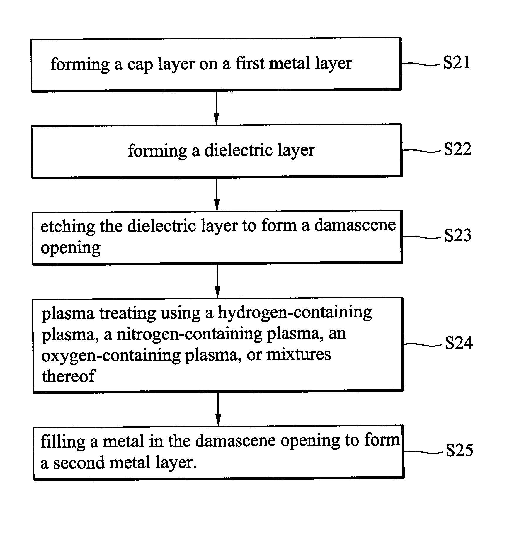
An object of the present invention is to solve the above-mentioned problems and provide a process for forming a metal damascene structure. After the damascene opening etching, the present invention performs a special plasma treatment to remove the residual impurities. Thus, peeling of the intermetal dielectric (IMD) layer due to the remaining impurities is solved. Moreover, the present invention can pass the stress migration and electro-migration tests. Moreover, yield and reliability are improved.
According to the present invention, after the first metal layer is formed and before the dielectric layer is formed, a cap layer can be formed on the first metal layer. Thus, the plasma treatment can act to repair the bonding between the first metal layer and the cap layer.
According to a first preferred embodiment of the present invention, etching of the damascene opening is conducted by fluorine containing plasma or a chlorine-containing plasma, and the plasma treatment uses hydrogen-containing plasma. For example, hydrogen (H2) plasma, ammonia (NH3) plasma, H2 / NH3 plasma, or H2 / N2 plasma can be used. The hydrogen bond of the hydrogen-containing plasma is ionized to form ionized hydrogen atoms. These ionized hydrogen atoms can deoxidize undesired copper oxide and react with free fluorine or chlorine. Therefore, dielectric layer peeling due to residual fluorine or chlorine can be eliminated.
According to a second preferred embodiment of the present invention, the cap layer is nitride and the plasma treatment uses nitrogen-containing plasma. For example, nitrogen (N2) plasma, ammonia (NH3) plasma, H2 / N2 plasma, or H2 / NH3 plasma can be used. The nitrogen-containing plasma can repair the bonding between the first metal layer and the cap layer (nitride). Thus, the first metal layer and the cap layer have good adhesion, and peeling of the dielectric layer can be eliminated.
According to a third preferred embodiment of the present invention, the photoresist mask for the damascene opening etching contains carbon, and the plasma treatment uses oxygen-containing plasma such as N2O plasma or oxygen (O2) plasma. The oxygen-containing plasma can react with the remaining carbon, thus preventing formation of blisters due to remaining carbon.

Problems solved by technology

However, integration of semiconductors has rapidly increased, and the conductivity of aluminum and aluminum alloy can no longer satisfy the speed requirements for semiconductor devices.
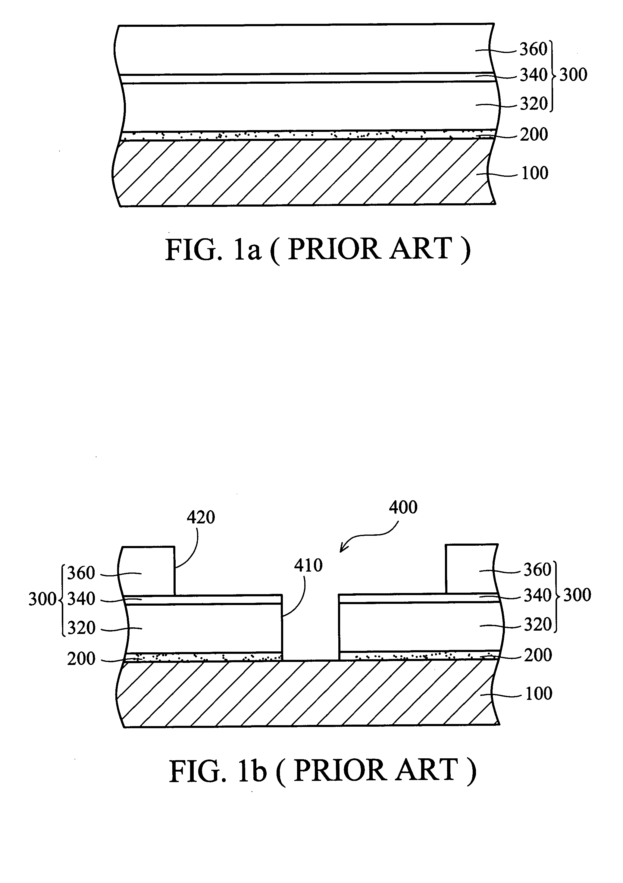
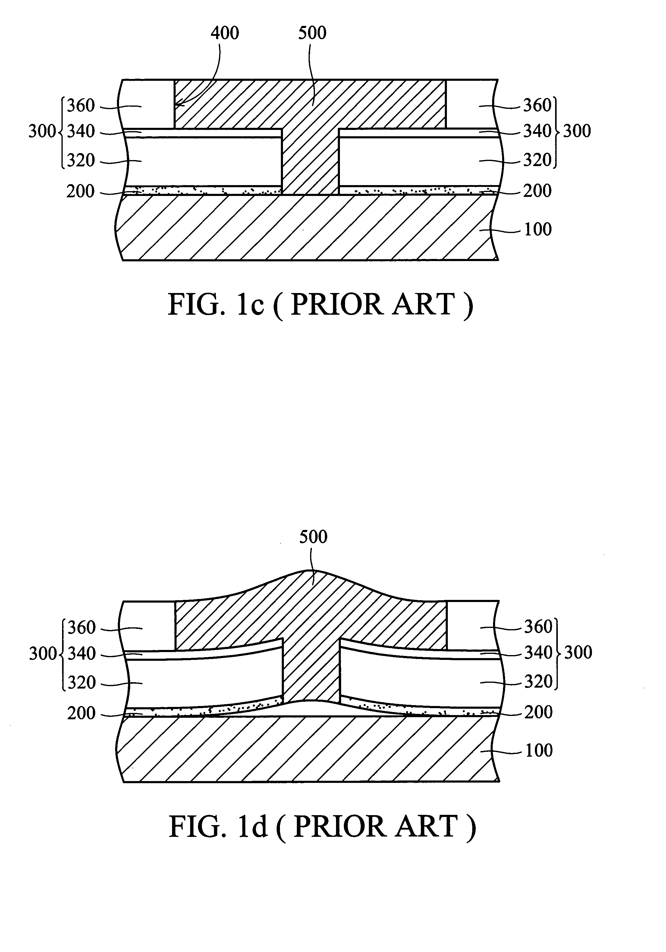
The peeling via will not only reduce yield, but also diminish reliability.
Moreover, severe electromigration (EM) and stress migration (SM) problems occur.
The peeling via issue, however, continues to be a problem.

Method used


Image

  • Process for forming metal damascene structure to prevent dielectric layer peeling
  • Process for forming metal damascene structure to prevent dielectric layer peeling
  • Process for forming metal damascene structure to prevent dielectric layer peeling

Examples


example

According to the above-mentioned process of the present invention, after the dielectric layer was etched to form a damascene opening, a plasma treatment using H2 / NH3 plasma was performed. Then, copper was filled in the damascene opening to complete metallization and obtain a testing structure shown in FIGS. 4a and 4b. The copper lines are capped by SiN cap layers (not shown).

FIG. 4a is a top view and FIG. 4b is a side view of the testing structure for electromigration (EM) and stress migration (SM). The testing structure includes four levels of metal. Symbol 61 indicates a metal line (the first level), and symbols 621 and 622 indicate metal pads (the second level), in which the pad 621 connects the metal line 61 via a plug 611 and the pad 622 connects the metal line 61 via a plug 612. Symbols 631 and 632 indicate metal pads (the third level), and symbol 64 indicates a metal line (the fourth level), in which the pad 631 connects the metal line 64 via a plug 633 and the pad 632 conn...


PUM


Abstract

A process for forming a metal damascene structure. First, a cap layer is formed on a first metal layer, and a dielectric layer is formed on the cap layer. Next, the dielectric layer is etched to form a damascene opening. Next, hydrogen-containing plasma, nitrogen-containing plasma, oxygen-containing plasma, or a mixture thereof is used to perform the plasma treatment. Next, a metal is filled in the damascene opening to form a second metal layer. Peeling of the dielectric layer due to remaining impurities is eliminated by the plasma treatment after etching of the damascene opening.

Description

BACKGROUND OF THE INVENTION 1. Field of the Invention The present invention relates to a process for forming a metal damascene structure, and more particularly to a process for forming a metal damascene structure to prevent peeling of the dielectric layer, using a special plasma treatment after damascene opening etching. 2. Description of the Prior Art Due to their high degree of conductivity, aluminum (Al) and aluminum alloy have been important as conductive materials in the development of the integrated circuit (IC). However, integration of semiconductors has rapidly increased, and the conductivity of aluminum and aluminum alloy can no longer satisfy the speed requirements for semiconductor devices. Therefore, copper (Cu) is gradually replacing aluminum as a conductive material, because of its lower resistance and better reliability. In addition, copper is more resistant than aluminum to electromigration. Therefore, in devices with design rule beyond 0.13 μm technology, copper...

Claims


Application Information

Patent Timeline
IPC IPC(8): H01L21/28H01L21/306H01L21/3065H01L21/311H01L21/3205H01L21/4763H01L21/768
CPCH01L21/02046H01L21/31116H01L21/76838H01L21/76814H01L21/76807
Inventor WANG, MING-TSONGSU, DI-SHIYANG, CHIA-MINGTSAI, CHING-MING
Owner TAIWAN SEMICON MFG CO LTD
Learn More