High intensity discharge lamp ballast apparatus
- Summary
- Abstract
- Description
- Claims
- Application Information
AI Technical Summary
Benefits of technology
Problems solved by technology
Method used
Image
Examples
embodiment 1
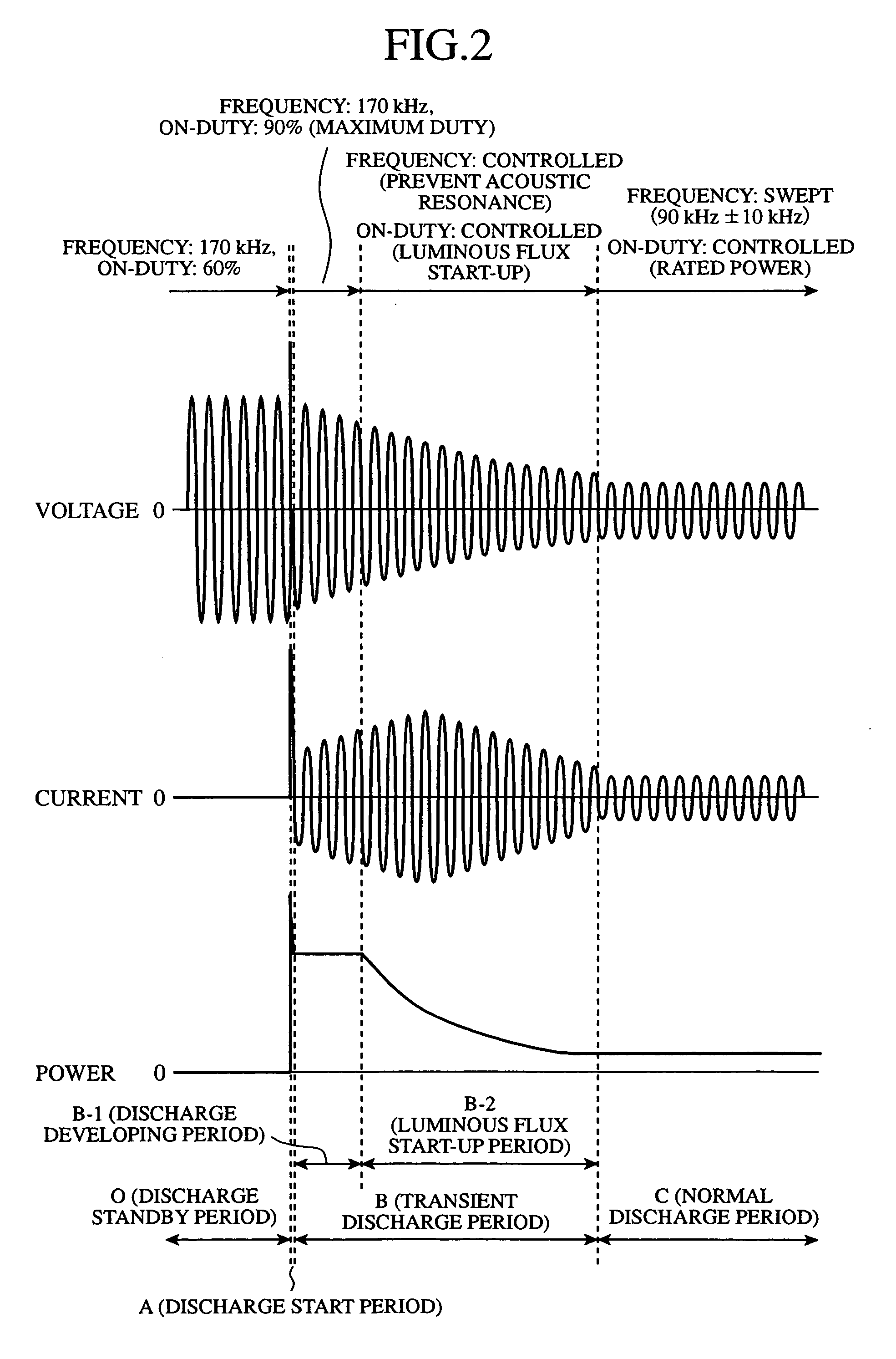
[0026]FIG. 1 is a circuit diagram showing a configuration of a metal halide lamp ballast apparatus 100 (high intensity discharge lamp ballast apparatus) of an embodiment 1 in accordance with the present invention. As shown in FIG. 1, the metal halide lamp ballast apparatus 100 includes a DC power supply 10 such as a battery, a smoothing capacitor 20, a DC-AC inverting booster circuit 30 (DC-AC inverter), a first resonance circuit 40, a high voltage pulse generating circuit 50, a second resonance circuit 60, and a ballast control circuit 70.
[0027] The DC-AC inverting booster circuit 30 has a FET (Field Effect Transistor) 31 and a FET 32 (switching element), and a DC-AC converter transformer 33 (transformer). The FETs 31 and 32 are each turned on and off in response to a pulse signal fed from the ballast control circuit 70 to their gates. Thus, the current flowing through the primary winding 34 of the DC-AC converter transformer 33 is altered so that a rectangular wave voltage is gen...
PUM
 Abstract
Description
Claims
Application Information
 - R&D
- Intellectual Property
- Life Sciences
- Materials
- Tech Scout
- Unparalleled Data Quality
- Higher Quality Content
- 60% Fewer Hallucinations
Browse by: Latest US Patents, China's latest patents, Technical Efficacy Thesaurus, Application Domain, Technology Topic, Popular Technical Reports.
© 2025 PatSnap. All rights reserved.Legal|Privacy policy|Modern Slavery Act Transparency Statement|Sitemap|About US| Contact US: help@patsnap.com


