Incorporation of carbon in silicon/silicon germanium epitaxial layer to enhance yield for Si-Ge bipolar technology

a silicon germanium and epitaxial layer technology, applied in the field of silicon germanium (sige) bipolar transistors, can solve the problems of dislocation between the collector and the emitter region, and the only sige region is effective in reducing pipe shorts

Inactive Publication Date: 2005-03-10
GLOBALFOUNDRIES US INC
View PDF46 Cites 34 Cited by
  • Summary
  • Abstract
  • Description
  • Claims
  • Application Information

AI Technical Summary

Benefits of technology

[0008] One object of the present invention is to provide a method of fabricating a SiGe bipolar transistor in which the formation of dislocations between the emitter and collector regions have been substantially suppressed therefore avoiding the problem of bipolar pipe, e.g., CE, shorts.

Problems solved by technology

A major problem with bipolar SiGe transistors of the type illustrated in FIG. 1 is the presence of dislocations between the collector and emitter regions.
Despite being able to suppress the diffusion of boron, this prior art method which forms C over the base in the SiGe region only is not effective in reducing pipe shorts.

Method used


Image

  • Incorporation of carbon in silicon/silicon germanium epitaxial layer to enhance yield for Si-Ge bipolar technology
  • Incorporation of carbon in silicon/silicon germanium epitaxial layer to enhance yield for Si-Ge bipolar technology
  • Incorporation of carbon in silicon/silicon germanium epitaxial layer to enhance yield for Si-Ge bipolar technology

Examples


Embodiment Construction

[0030] The present invention which is directed to a method of continuously incorporating C into the lightly doped Si collector region as well as the SiGe base layer and a SiGe bipolar structure produced therefrom will now be described in more detail by referring to the drawings that accompany the present invention.

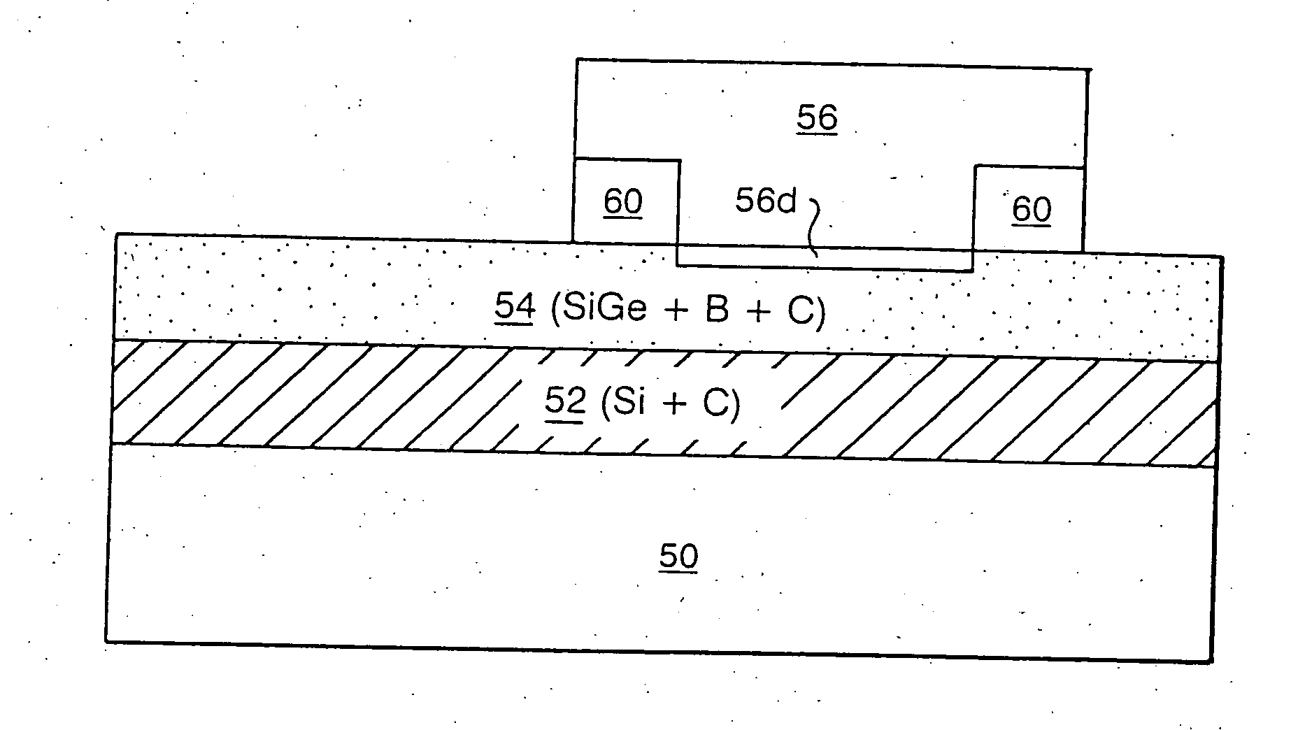
[0031] Reference is first made to FIG. 4 which is a cross-sectional illustration of a fragment of the inventive SiGe bipolar transistor. Specifically, the SiGe bipolar transistor shown in FIG. 4 comprises a collector region 52 of a first conductivity type (n or p-type doped) which is formed on substrate 50. On top of a portion of collector region 52 is SiGe base region 54 which includes emitter region 56 and emitter diffusion 56d. Region 60 denote an insulator. The SiGe base region is characterized as being doped with B. It should be noted that the bipolar transistor shown in FIG. 4 represents only a fragment of the bipolar transistor. For simplicity, the drawings have om...


PUM


Abstract

A SiGe bipolar transistor containing substantially no dislocation defects present between the emitter and collector region and a method of forming the same are provided. The SiGe bipolar transistor includes a collector region of a first conductivity type; a SiGe base region formed on a portion of said collector region; and an emitter region of said first conductivity type formed over a portion of said base region, wherein said collector region and said base region include carbon continuously therein. The SiGe base region is further doped with boron.

Description

FIELD OF THE INVENTION [0001] The present invention relates to bipolar transistors, and more particularly to a silicon germanium (SiGe) bipolar transistor which includes a lightly doped Si collector region and a SiGe base region that include carbon, C, continuously incorporated throughout the collector and SiGe base regions. A method of continuously incorporating C into the lightly doped Si collector region and SiGe base region of a SiGe bipolar transistor is also disclosed herein. The term SiGe is used herein to denote silicon-germanium alloys, i.e., Si1-xGex. BACKGROUND OF THE INVENTION [0002] Significant growth in both high-frequency wired and wireless markets has introduced new opportunities where compound semiconductors such as SiGe have unique advantages over bulk complementary metal oxide semiconductor (CMOS) technology. With the rapid advancement of epitaxial-layer pseudomorphic SiGe deposition processes, epitaxial-base SiGe heterojunction bipolar transistors have been integ...

Claims


Application Information

Patent Timeline
Patent Type & Authority Applications(United States)
IPC IPC(8): H01L21/331H01L29/737
CPCH01L21/02381H01L21/02447H01L21/02529H01L21/02532H01L29/7378H01L21/0262H01L29/1004H01L29/161H01L29/66242H01L21/02579H01L29/737
Inventor CHU, JACK OONCOOLBAUGH, DOUGLAS DUANEDUNN, JAMES STUARTGREENBERG, DAVID R.HARAME, DAVID L.JAGANNATHAN, BASANTHJOHNSON, ROBB ALLENLANZEROTTI, LOUIS D.SCHONENBERG, KATHRYN TURNERWUTHRICH, RYAN WAYNE
Owner GLOBALFOUNDRIES US INC
Why Eureka
Try Eureka