Semiconductor device and manufacturing method

A manufacturing method and semiconductor technology, applied in the direction of semiconductor/solid-state device manufacturing, semiconductor devices, electric solid-state devices, etc., can solve the problems of not being practical, increasing costs, dislocations, etc., and achieve the effect of excellent drain current characteristics

Inactive Publication Date: 2005-03-09
HITACHI LTD
View PDF1 Cites 4 Cited by
  • Summary
  • Abstract
  • Description
  • Claims
  • Application Information

AI Technical Summary

Problems solved by technology

[0004] However, as described above, if materials with different crystal lattice constants are epitaxially grown to match their lattices, the deformation energy generated in the crystal is large, and when the film thickness is equal to or greater than a certain critical film thickness, there may be a The problem of dislocations in crystallization, in the manufacturing process of semiconductor devices such as LSI, introduces new manufacturing equipment along with the introduction of silicon germanium materials that are generally not available, which increases the cost, so the above method has not been practical.

Method used


Image

  • Semiconductor device and manufacturing method
  • Semiconductor device and manufacturing method
  • Semiconductor device and manufacturing method

Examples


Embodiment Construction

[0048] Hereinafter, examples of the present invention will be described. In addition, this invention is not limited to the following Example, It can apply to another aspect.

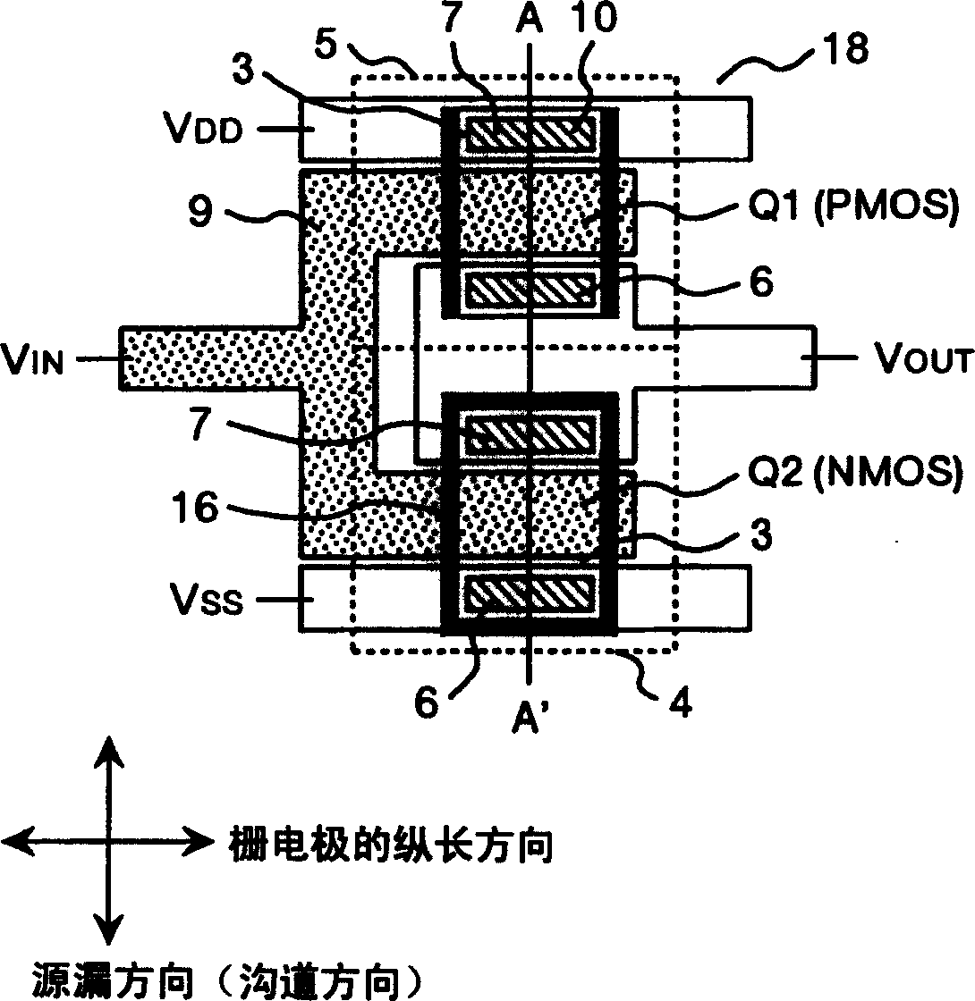
[0049] use below figure 1 The first embodiment of the present invention will be described. figure 1 is the inverter circuit diagram of this embodiment, figure 2 It is a layout diagram. image 3 yes means figure 1 Sectional view of A-A'.

[0050] like figure 2 As shown, the present embodiment has a p-channel field effect transistor Q1, an n-channel field effect transistor Q2, and wirings electrically connecting these transistors.

[0051] The n-channel type field effect transistor Q2 formed on the substrate (sub1) 1 consists of an n-type source (soce1) 6, a drain (drain1) 7, and a gate electrode formed on a p-type well layer (pwell) 4. (poly-Si) 9, gate oxide film (gato-ox) 8. And the p-channel type field effect transistor Q1 is formed on the n-type well layer (pwell) 5 by the p-type source (...


PUM


Abstract

The object of the present invention is to provide a semiconductor device comprising an n-type channel field effect transistor and a p-type channel field effect transistor, which has a high degree of reliability and excellent drain current characteristics. The gist of the invention for attaining the object resides in disposing a silicon nitride film to the side wall of a trench for an active region in which the n-type channel field effect transistor is formed and disposing the silicon nitride film only in the direction perpendicular to the channel direction to the sidewall of the trench for the active region of the p-type channel field effect transistor. According to the present invention, a semiconductor device comprising an n-type channel field effect transistor and a p-type channel field effect transistor of excellent current characteristics can be provided.

Description

technical field [0001] The invention relates to a semiconductor device, especially a semiconductor device with an n-channel field effect transistor and a p-channel field effect transistor. Background technique [0002] In recent years, with the development of information communication devices, the processing capability of semiconductor devices such as large scale integration (LSI) has become increasingly strict, and the operation speed of transistors has been increased. In particular, complementary field effect transistors composed of n-channel field effect transistors and p-channel field effect transistors are widely used because of their low power consumption, but their high-speed development is mainly due to the miniaturization of the structure. Supported by advances in photolithography for processing semiconductor components. However, the minimum processing size (minimum processing size of the gate electrode) required recently has become below the wavelength level of li...

Claims


Application Information

Patent Timeline
Patent Type & Authority Applications(China)
IPC IPC(8): H01L21/76H01L21/762H01L21/822H01L21/8238H01L27/04H01L27/08H01L27/092H01L27/10
CPCH01L21/823807H01L29/7842H01L21/823878H01L29/7846H01L21/76224H01L21/8238
Inventor 石塚典男熊谷幸博三浦英生池田修二竹田敏文太田裕之
Owner HITACHI LTD
Why Eureka
Try Eureka