Group III nitride photonic devices on silicon carbide substrates with conductive buffer interlayer structure

a technology of conductive buffer and nitride, which is applied in the direction of lasers, transistors, active medium materials, etc., can solve the problems of electrically insulating characteristics, certain disadvantages, and limited materials which can work well to support group iii nitride active layer devices, so as to avoid cracking

Inactive Publication Date: 2002-01-24
CREE INC
View PDF0 Cites 89 Cited by
  • Summary
  • Abstract
  • Description
  • Claims
  • Application Information

AI Technical Summary

Benefits of technology

[0013] Therefore, it is an object of the present invention to produce photonic devices and their wafer precursors, with a Group III nitride active layer, a conductive silicon carbide substrate, and a conductive buffer layer, but that avoids the cracking and other problems that have to date hindered such combinations of materials and layers.
[0016] In another aspect, the buffer layer includes a plurality of discrete crystal portions selected from the group consisting of gallium nitride and indium gallium nitride on the surface of the silicon carbide substrate for minimizing or eliminating the heterobarrier between silicon carbide and aluminum gallium nitride buffer structure.
[0036] FIG. 2 shows the manner in which the present invention provides for a more compact device. In FIG. 2 the device is broadly designated at 30, and includes a conductive silicon carbide substrate 31, a back contact 32, an active layer 33 and a conductive buffer structure 34, along with a top contact 35. The invention thus eliminates the shorting contacts (typically shorting ring contacts) 25 of the device of FIG. 1. As a result, the device 30 is easier to manufacture and more efficient in operation. It will be understood that the active layer 33 as discussed herein can represent a device with a single p-n junction, a single or double p-n heterojunction or a p-n junction quantum well structure. Such structures are described in a number of prior U.S. patents including Nos. 5,393,993 and 5,592,501, and will not be otherwise discussed in detail herein other than to further illustrate the present invention.
[0042] FIG. 11 is another 10.times. SEM photograph and illustrates a grid pattern of grooves in the epitaxial layer. In comparison with FIG. 10, the surface shown in FIG. 11 is relatively free of cracking defects.
[0052] FIGS. 16 and 17 illustrate another embodiment of the invention. In general, in schematic fashion, the overall structure is again illustrated by FIG. 2 and comprises the silicon carbide substrate 31, the photonic diode 33 and the buffer layer 34. In this embodiment, however, the buffer layer is aluminum gallium nitride rather than gallium nitride or indium gallium nitride. This embodiment includes a plurality of discrete crystal portions that appear as the white colored dots in FIGS. 16 and 17. The discrete crystal portions are selected from the group of gallium nitride and indium gallium nitride and are on the surface of the silicon carbide substrate for minimizing or eliminating the heterobarrier between the silicon carbide substrate 31 and the aluminum gallium nitride buffer structure 34.
[0063] As set forth in the structural aspects of the invention, the method comprises forming discrete crystal portions of a size and in an amount that is sufficient to minimize or eliminate the heterobarrier, but less than sizes or amounts that would detrimentally affect or destroy the function of any resulting diode device built on the silicon carbide substrate. In particular the invention provides a robust structure that can withstand normally expected levels of electrostatic discharge.

Problems solved by technology

Because of the differences in the structural characteristics of semiconductor materials, however, particularly their crystal lattice structures, the materials which will workably support Group III nitride active layer devices are somewhat limited.
Sapphire (Al.sub.2O.sub.3) provides a relatively close lattice match to Group III nitrides, but also suffers certain disadvantages, the most limiting of which is its electrically insulating character.
Thus, when Group III nitride active and buffer layers (i.e., the intermediate layers that provide a crystal structure transition from the substrate to the active layer) are built on sapphire, the sapphire cannot be used as a conductive pathway to the active portions of the device.
This limits the type of devices that can be designed and produced on sapphire, and in particular limits the ability to form "vertical" devices in which the device contacts can be placed on opposite surfaces of the device with a direct conductive path through the substrate, buffers, and active layer. and the other contacts on the opposite of the device.
Aluminum nitride is, however, insulating rather than conductive.
In turn, eliminating the shorting contact reduces the epitaxial layer thickness, decreases the number of fabrication steps required to produce devices, reduces the overall chip size, and increases the device efficiency.
Nevertheless, although these conductive buffer materials offer these advantages, their crystal lattice match with silicon carbide is less satisfactory than is that of aluminum nitride.
Accordingly, when epitaxial buffer layers of gallium nitride, aluminum gallium nitride, or combinations thereof are grown on silicon carbide substrates, they tend to produce excessive cracking in subsequent epilayers that are required for photonic devices such as light-emitting diodes or laser diodes.

Method used


Image

  • Group III nitride photonic devices on silicon carbide substrates with conductive buffer interlayer structure
  • Group III nitride photonic devices on silicon carbide substrates with conductive buffer interlayer structure
  • Group III nitride photonic devices on silicon carbide substrates with conductive buffer interlayer structure

Examples


Embodiment Construction

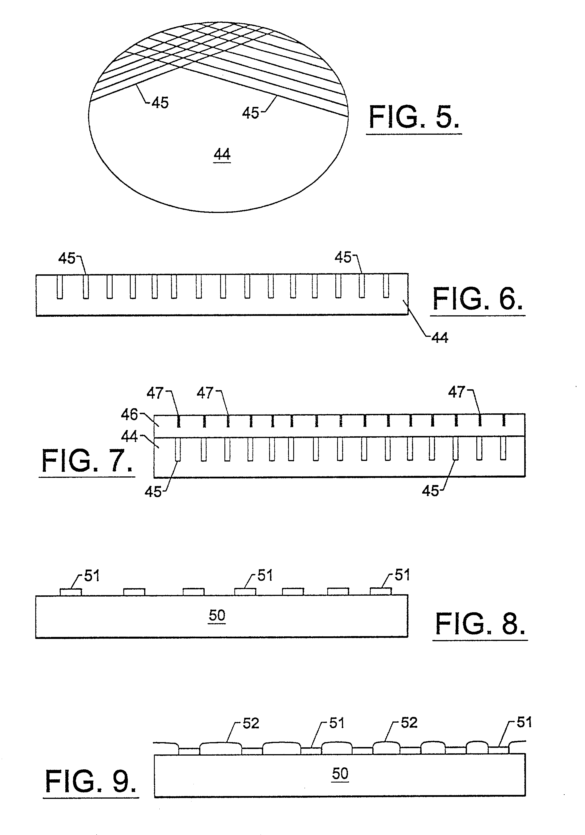
[0066] In a current process for producing conductive buffer LEDs and Laser Diodes, GaN dots are first deposited. The purpose of the GaN dots is to decrease the barrier between the SiC substrate and the Si-doped AlGaN buffer layer. This is done at considerably lower temperatures than are used for the other epitaxial layers in the structure. The size and density of the dots are shown in FIGS. 16 and 17. It is important to keep the dots relatively small so the electrostatic discharge will not be adversely affected. The GaN dots are deposited in about 6 seconds, and then "capped" with Si-doped Al.sub.0.10Ga.sub.0.90N for about 15 seconds. The purpose of this cap is to prevent the dissociation of the GaN dots upon heating. In this material system, adding any Al to GaN, i.e., Al.sub.(1-x)Ga.sub.(X)N decreases the dissociation rate of the material because AlGaN is more stable than GaN in an NH.sub.3 / H.sub.2 atmosphere. After the capping of the dots, the temperature is then ramped up to the...


PUM

PropertyMeasurementUnit
sizeaaaaaaaaaa
diameteraaaaaaaaaa
diameteraaaaaaaaaa

Abstract

An optoelectronic device with a Group III Nitride active layer is disclosed that comprises a silicon carbide substrate; an optoelectronic diode with a Group III nitride active layer; a buffer structure selected from the group consisting of gallium nitride and indium gallium nitride between the silicon carbide substrate and the optoelectronic diode; and a stress-absorbing structure comprising a plurality of predetermined stress-relieving areas within the crystal structure of the buffer structure, so that stress-induced cracking that occurs in the buffer structure occurs at predetermined areas rather than elsewhere in the buffer structure.

Description

[0001] This application is a continuation of copending U.S. application Ser. No. 08 / 944,547, filed Oct. 7, 1997.[0002] This invention relates to photonic devices in wide bandgap materials, and in particular relates to photonic devices formed with Group III nitride active layers on silicon carbide substrates.[0003] The semiconductor materials with wide bandgaps such as diamond, silicon carbide, and gallium nitride have become of significant interest in recent years because their wide bandgap characteristics provide them with the capability to emit light of higher energy (with correspondingly higher frequency and shorter wavelength) than do other semiconductor materials such as silicon or gallium arsenide. In particular, silicon carbide, gallium nitride, and certain other Group III nitrides have bandgaps large enough to produce visible light throughout the visible spectrum, including the higher-energy blue portion. They thus provide the basis for semiconductor lasers and light emittin...

Claims


Application Information

Patent Timeline
Patent Type & Authority Applications(United States)
IPC IPC(8): H01L21/20H01L33/00
CPCH01L21/02378H01L21/02458H01L21/02513H01L21/0254H01L21/02642H01L33/007
Inventor EDMOND, JOHN ADAMKONG, HUA-SHUANGDOVERSPIKE, KATHLEEN MARIELEONARD, MICHELLE TURNER
Owner CREE INC
Why Eureka
Try Eureka