Soldered product

a soldering method and soldering technology, applied in the direction of solid-state devices, surface reaction electrolytic coating, printed circuit assembling, etc., can solve the problems of insufficient strength of soldering, difficulty in cleaning operation, and increasing restrictions on the use of cleaning agents

Inactive Publication Date: 2001-09-20
DENSO CORP
View PDF0 Cites 3 Cited by
  • Summary
  • Abstract
  • Description
  • Claims
  • Application Information

AI Technical Summary

Benefits of technology

[0010] Accordingly, unlike flux, the auxiliary connecting material physically disperses the oxide film on the surface of the main connecting material without chemically dissolving it, which makes it possible for the base member and the connected member to be electrically and mechanically joined securely. Herein, in case the auxiliary connecting material comprises an insulating material having no functional group, the insulation quality thereof is prevented from deteriorating after the soldering operation, and thus it will not cause the insulation quality around an electrode joint to be reduced even if it is left in the periphery of the joint.
[0011] The main connecting material may be coated on at least one of connection surfaces of either the base member or the connected member. In this case, as the auxiliary connecting material, a material capable of vaporizing around at the melting point of the main connecting material may be selected to cause the auxiliary connecting material to be vaporized during the heat treating step. By means of this, the oxide film can be destroyed during the heat treating step to electrically and mechanically connect the base member and the connected member with high reliability, and the auxiliary connecting material can be vaporized away after soldering as well.
[0012] Also, as the auxiliary connecting material, a material mainly composed of such material whose boiling point is greater than the melting point of the main connecting material and whose vapor pressure is 1 / 100 or over of the external pressure at a maximum temperature during the heat treating step may be selected to cause the auxiliary connecting material to be cubically expanded during the heat treating step. By means of this, the auxiliary connecting material existing around the joint portion will get into a boiling condition, undergoing an abrupt cubical expansion. The energy generated by this cubical expansion will physically disperse and destroy the oxide film which is staying as formed without being dissolved on the surface of the main connecting material, thereby causing the non-oxidized section to be exposed to electrically and mechanically connect the base member and the connected member with high reliability.
[0013] Furthermore, it may be possible for the main connecting material and the auxiliary connecting material to be kneaded and formed into a paste-like condition to be applied to the joint portion between the base member and the connected member. Besides enabling the base member and the connected member to be electrically and mechanically connected in a good condition, the formed paste also allows the base member and the connected member to be fixed tentatively through the paste, which makes it easier for them to be mounted.

Problems solved by technology

The flux has to be removed by cleaning after a connecting operation is finished since it is corrosive.
In view of the environmental problems, however, there has been increasing restrictions imposed on the use of cleaning agents which contain CFCs (chlorofluorocarbons).
A cleaning operation is sometimes difficult to be performed in the case of a soldering operation which has to be executed inside a package.
In the cases like these where low active flux is used or soldering operations are performed without using flux, it is difficult to secure a sufficient area for connection due to the effect of an oxide film on the surface of solder, which has given rise to such problems as the soldering being insufficient in strength and the connection being low in reliability, or voids occurring inside solder.
Although the above-mentioned technique shows a method for preventing an oxide film from being formed, and for keeping and using solder under a condition in which there is no penetration of water, but it does not deal with soldering which has to be performed under a condition in which there is an oxide film formed on solder.
In other words, soldering cannot be executed unless terminals have been solder-plated in advance as in the case of connections between terminals, and in the event of solder surface being oxidized, solder coated with paraffine wax cannot be used for connections between terminals.

Method used


Image

  • Soldered product
  • Soldered product
  • Soldered product

Examples


first embodiment

[0025] A description shall be given below of this invention with reference to several embodiments thereof.

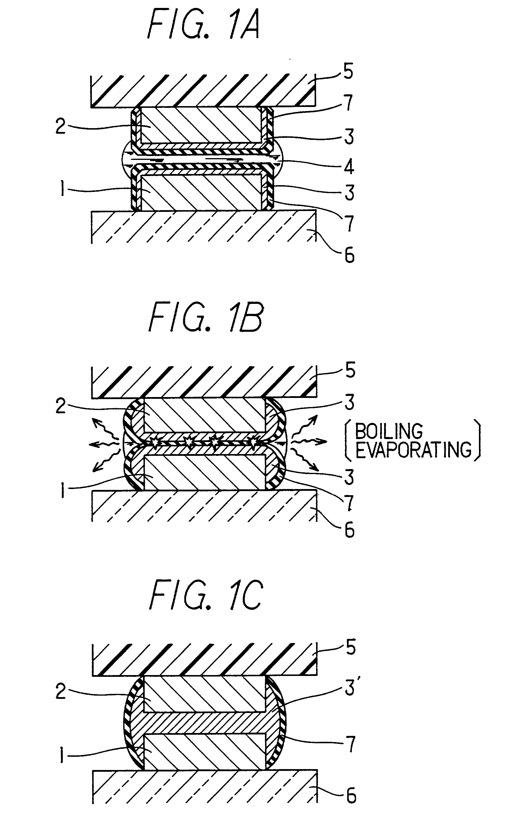
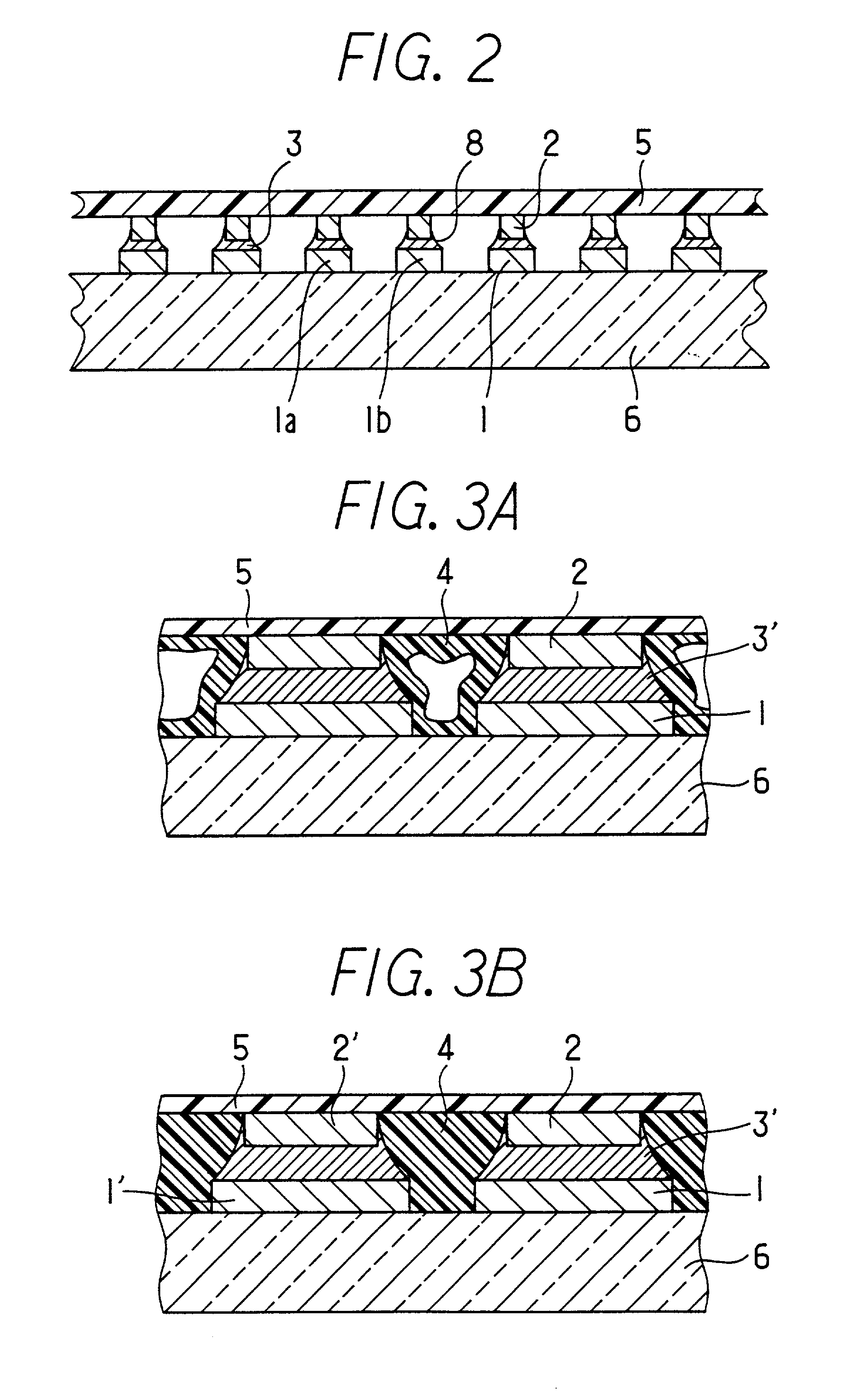
[0026] FIGS. 1A to 1C are typical explanatory drawings showing the cases in sequential order in which a copper terminal (the first connection surface) 1 which is formed on a rigid substrate 6 made of glass or glass epoxy and a copper terminal (the second connection surface) 2 which is provided on a flexible substrate (a connected member) 5 made of plastic film are connected by means of soldering. FIG. 2 is a schematic sectional view showing a disposition of the copper terminals 1 and 2.

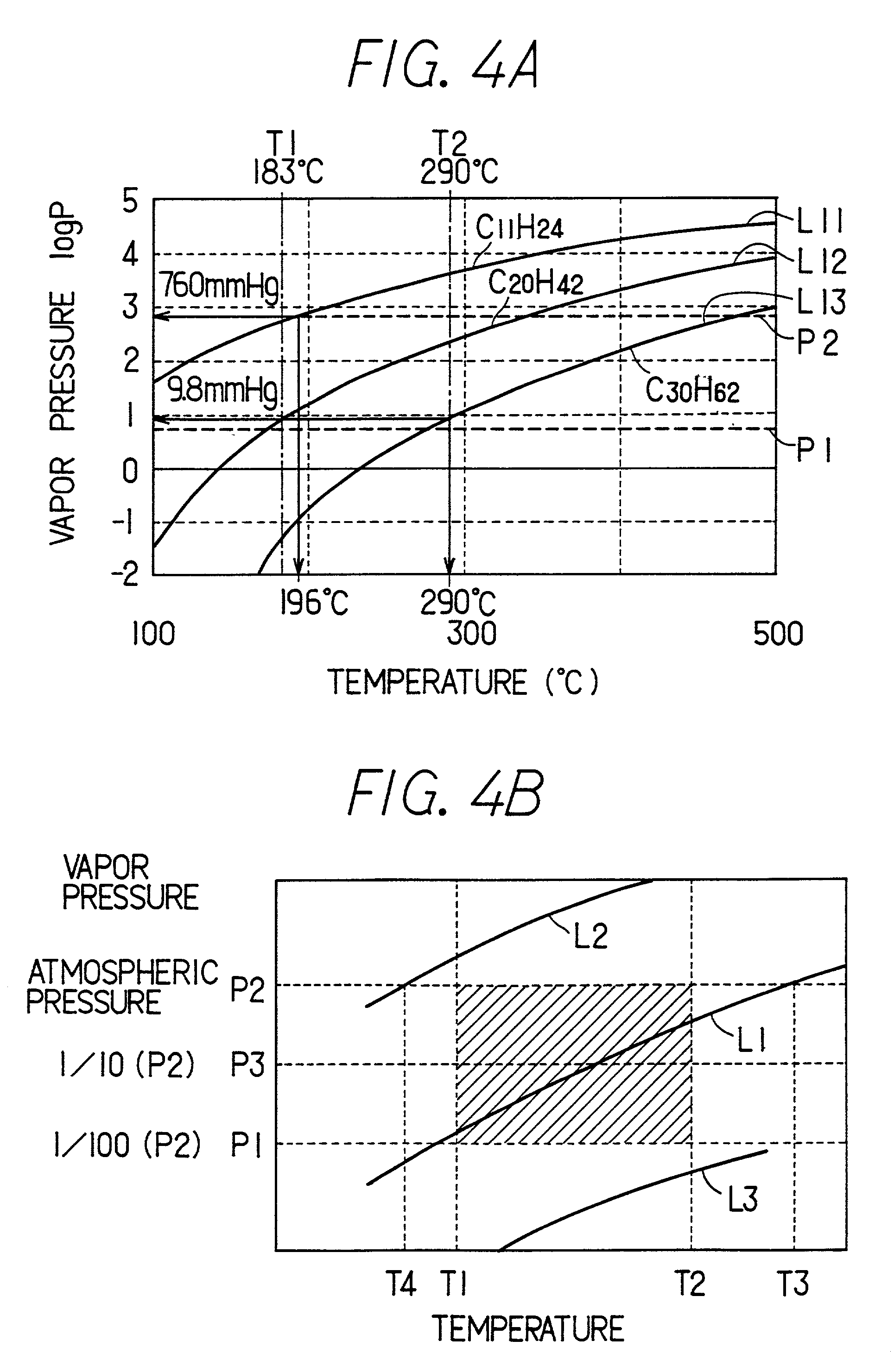
[0027] In FIG. 1A, solder (main connecting material) 3 has been applied beforehand on the surfaces of each copper terminal 1 and 2, and the surface of the solder 3 is covered with an oxide film 7 before being connected. FIG. 1A shows the copper terminals 1 and 2 in that condition placed one on top of the other so as to be connected. Before placing the terminals one upon the other, an auxiliary con...

second embodiment

[0057] FIG. 5 is a schematic diagram of a case in which this invention is applied to an outlet terminal 51 on a plane display panel of an EL display or a liquid crystal display. A description shall be given on an EL display 50. The EL display 50 is a display illuminated when voltage is applied to a luminous layer formed on a glass substrate 52. The voltage is applied by electrodes disposed in a matrix configuration. The EL display 50 has terminals, that is, the outlet terminals 51, for applying voltage from outside to electrodes disposed in a matrix configuration, which are formed around the periphery of the glass substrate 52 in a numerous microscopic array. This outlet terminal 51 is electrically connected to a control substrate 54, an external circuit, through a flexible substrate (FPC) 53.

[0058] As in the case of the first embodiment, soldering was performed to the outlet terminal 51 by using n-tetradecane. The result of the soldering is the same as shown in the sectional struct...

third embodiment

[0062] FIG. 6 is a typical sectional view showing the connection structure between a circuit substrate 13 and a QFP (Quad Flat Package) type flat package 12 having an integrated circuit inside the package made up of resin material, with leads 17 coming from the four sides thereof.

[0063] On the circuit substrate 13 are provided connecting terminals 14 at a pitch of 0.6 mm. The connecting terminals 14 are plated with eutectic solder of a composition of Sn 60 wt %- Pb 40 wt %. They are further coated with flux as an auxiliary connecting material, which is composed of abietic acid 10 wt %, adipic acid 0.05 wt %, n-tetradecane 10 wt % and the rest of organic solvent (not shown in the figure). The lead 17 of the flat package 12 is provided at a pitch of 0.6 mm. After mounting the flat package 12 on the circuit substrate 13 so that the lead 17 is located on the connecting terminal 14, the lead 17 is heated by means of a heater bar up to 220 to 290.degree. C., the solder 3 is re-flowed and ...


PUM

PropertyMeasurementUnit
thicknessaaaaaaaaaa
melting pointaaaaaaaaaa
temperatureaaaaaaaaaa

Abstract

A soldering method, which secures reliable joints without using flux, is disclosed. Soldering is performed using an auxiliary connecting material capable of physically destroying and dispersing an oxide film, which is naturally grown on the surface of a main connecting material such as solder or brazing between two terminals, to realize a reliable solder wetting (a state of the main connecting material being fused and mixed). For an auxiliary connecting material, hydrocarbon such as n-tetradecane (C14H30), for example, can be used. N-tetradecane boils between connection surfaces and cubically expands; energy generated therefrom physically disperses the oxide film and causes a fresh surface to be exposed; solders on both terminals are mixed; and an electrical and mechanical joint is securely achieved. The residue of the auxiliary connecting material is an insulating material, and therefore does not need cleaning. An excellent electrical joint which is moisture-resistant as well as highly reliable is attained.

Description

[0001] This application is based upon and claims the benefit of priority of the prior Japanese Patent Applications No. 7-91862, filed on Mar. 24, 1995, and No. 7-348710, filed on Dec. 18, 1995, and the prior U.S. application Ser. No. 08 / 620,212, filed Mar. 22, 1996 (now U.S. Pat. No. 5,669,548) and Ser. No. 08 / 908,457, filed Aug. 7, 1997, the contents all of which being incorporated herein by reference.[0002] 1. Field of the Invention[0003] The present invention relates to a soldering method. More specifically, the present invention relates to a method of electrically and mechanically connecting a substrate such as a rigid substrate and a flexible substrate, or a method of electrically and mechanically mounting on a substrate a connected member such as an IC (integrated circuit) chip, a discrete element and so on.[0004] 2. Description of Related Art[0005] In recent years, there have been growing demands, in the installation of electronic products, for techniques of connecting and mo...

Claims


Application Information

Patent Timeline
Patent Type & Authority Applications(United States)
IPC IPC(8): B23K1/015B23K35/14B23K35/36H05K1/14H05K3/34H05K3/36
CPCB23K1/015B23K35/3612B23K2201/40H01L24/13H01L24/16H01L24/81H01L2224/13099H01L2224/16H01L2224/81193H01L2224/81203H01L2224/81801H01L2924/01004H01L2924/01012H01L2924/01013H01L2924/01015H01L2924/01027H01L2924/01029H01L2924/0103H01L2924/01046H01L2924/01051H01L2924/01075H01L2924/01078H01L2924/01079H01L2924/01082H01L2924/01322H01L2924/14H05K3/3489H01L2924/01005H01L2924/01006H01L2924/01023H01L2924/01033H01L2924/01045H01L2924/01047H01L2924/0105H01L2924/014Y10S428/939H01L2224/131H01L2224/13111H01L2924/00014Y10T428/12514Y10T428/12556Y10T428/1259B23K2101/40
Inventor MIYAKE, TOSHIHIROKONDO, KOIIKURAHASHI, TAKASHIOKUMURA, NOZOMUTAKAGI, MAKOTO
Owner DENSO CORP
Why Eureka
Try Eureka