Semiconductor device having switching element suppressing potential variation

a technology of switching element and potential variation, which is applied in the direction of electronic switching, electrical apparatus construction details, pulse techniques, etc., can solve the problems of unstable gate potential high potential difference of the emitter, and malfunction of the switching element,

Active Publication Date: 2020-12-29
DENSO CORP
View PDF23 Cites 0 Cited by
  • Summary
  • Abstract
  • Description
  • Claims
  • Application Information

AI Technical Summary

Benefits of technology

[0008]The present disclosure, in view of these problems, provides an effective technology to keep the fluctuations of the potential of the emitter line of the switching elements low in a semiconductor device in which a plurality of switching elements are connected in parallel.
[0011]In the semiconductor device of the aforementioned embodiment, an emitter line which connects the emitter electrode of the switching elements with the anode electrode of the recirculation element is constituted by a plate-like member consisting of a conductive material. Since a plate-like member can shorten the path length compared to external wiring such as a bus bar, thus, the inductance is low. Therefore, even if the recovery current flows from a collector terminal to the emitter terminal during the recovery period of the recirculation element, the emitter potential difference generated in the emitter line can be kept low. Therefore, the gate potential of the switching elements can be stabilized by suppressing large fluctuations of the potential of the emitter line, and accordingly, the occurrence of malfunctions, etc., of the switching elements can be prevented. In this case, by keeping the inductance of the emitter line low, it is possible to increase the time change rate di / dt of the current, i.e., make the switching rate faster, and the loss reduction of the switching elements and chip size reduction can be ensured thereby.
[0012]Further, if constituted so that the distance from the emitter terminal to the recirculation element becomes no greater than the distance from the emitter terminal to the switching elements, the recirculation element can be arranged closer to the emitter terminal than the switching elements, or the recirculation element can set the separation distance for the emitter terminal in the same manner as the switching elements. In this case, the switching elements can be arranged in a position separated from the path of the recovery current which flows through the recirculation element to the emitter terminal during the recovery period of the recirculation element. Therefore, the effect of the recovery current can control the potential of the emitter line of the switching elements from fluctuating.
[0013]As stated above, according to the aforementioned embodiment, it is possible to keep the fluctuations of the potential of the emitter line of the switching elements low in the semiconductor device in which a plurality of switching elements are connected in parallel.

Problems solved by technology

When using the external wiring, the emitter potential difference is likely to become high.
Moreover, if the emitter potential difference becomes large and the potential of the emitter line, i.e., the reference potential of the gate potential greatly fluctuates, the gate potential of the switching elements is unstable which may cause a malfunction, etc., of the switching elements to occur.

Method used


Image

  • Semiconductor device having switching element suppressing potential variation
  • Semiconductor device having switching element suppressing potential variation
  • Semiconductor device having switching element suppressing potential variation

Examples


first embodiment

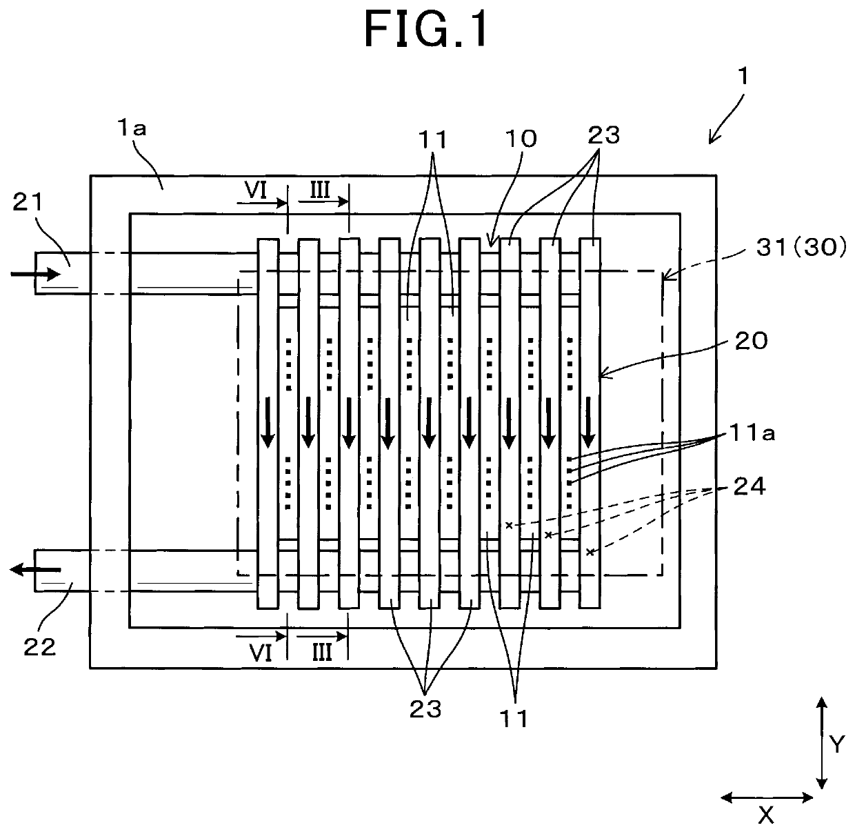
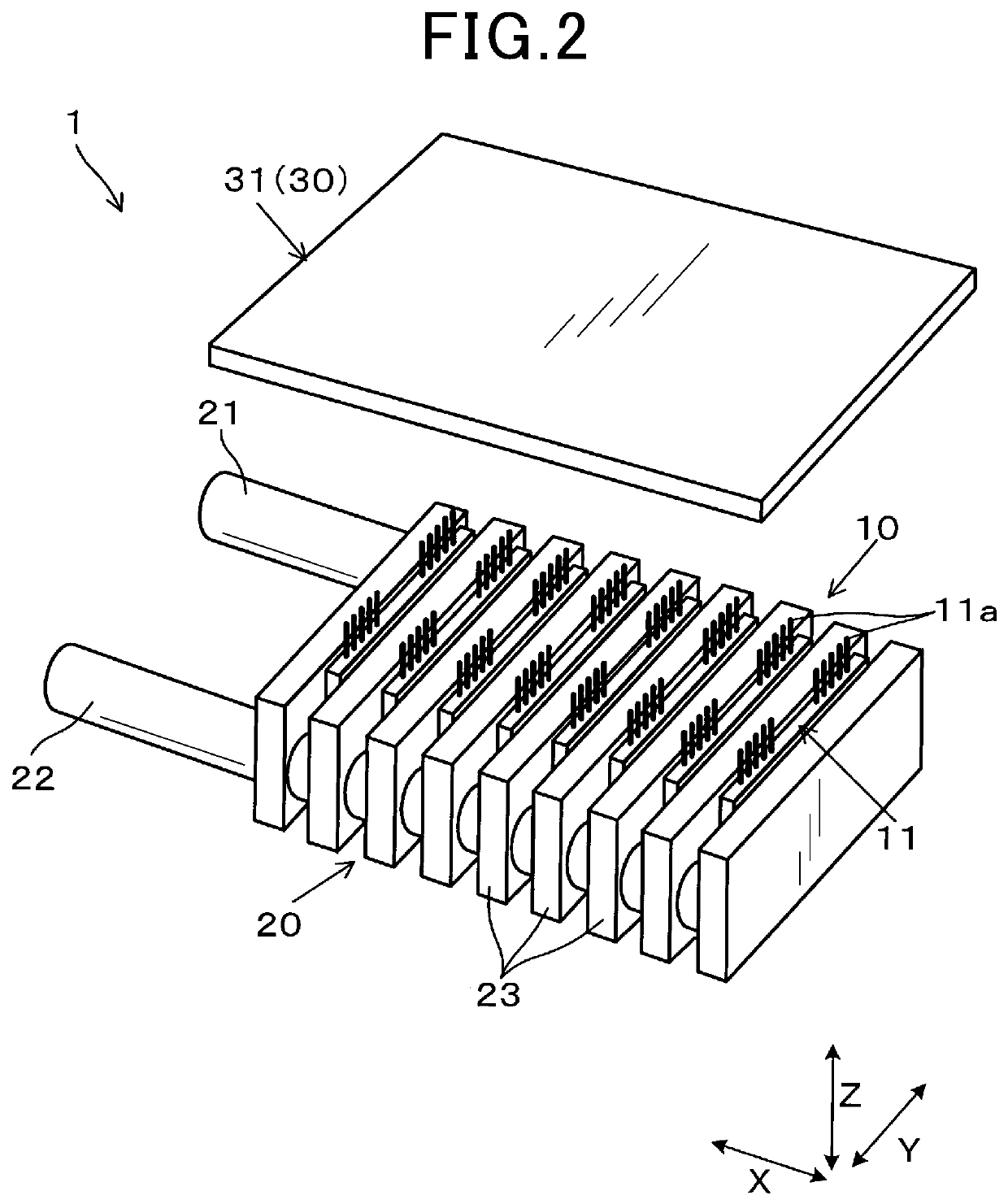
[0054]As shown in FIGS. 1 and 2, the power conversion device 1 comprises a plurality of elements including a semiconductor lamination unit 10 and a control circuit board 31 of a control part 30. These plurality of elements are housed in a space partitioned by a case 1a. The case 1a is an automobile component that is lightweight and requires high dimensional accuracy and is made by aluminum die casting method using aluminum.

[0055]The semiconductor lamination unit 10 comprises a plurality of the semiconductor devices 11 of the first embodiment, and a cooler 20 for cooling these plurality of the semiconductor devices 11. FIGS. 1 and 2 show eight semiconductor devices 11.

[0056]The cooler 20 comprises an inflow pipe 21 extending in the first direction X, an outflow pipe 22 extending in the first direction X, a plurality of cooling pipes 23 extending in the second direction Y and arranged at a predetermined interval with regards to the first direction X. FIGS. 1 and 2 show nine cooling pi...

second embodiment

[0095]As shown in FIG. 11, the semiconductor device 11 of the second embodiment is different from the semiconductor device 11 of the first embodiment regarding the arrangement of the emitter terminal 11n.

[0096]In the second embodiment, the emitter terminal 11n of the semiconductor device 11 extends to one side of the heat sink 17, i.e., from the right side to the second direction Yin FIG. 11.

[0097]The semiconductor device 11 is constituted so that the distance from the emitter terminal 11n to the recirculation element 15A becomes no greater than the distance from the emitter terminal 11n to the switching elements 14A.

Further, the semiconductor device 11 is constituted so that the distance from the emitter terminal 11n to the recirculation element 15B becomes no greater than the distance from the emitter terminal 11n to the switching element 14B.

[0098]The other configurations are the same as the first embodiment.

[0099]According to the second embodiment, even when the arrangement of ...

third embodiment

[0101]As shown in FIG. 12, the semiconductor device 11 of the third embodiment is different from the semiconductor device 11 of the first embodiment regarding the arrangement of both the collector terminal 11p and the emitter terminal 11n.

[0102]In the third embodiment, the collector terminal 11p of the semiconductor device 11 extends to one side of the heat sink 16, i.e., from the upper side in the third direction Z in FIG. 12. Further, the emitter terminal 11n extends to one side of the heat sink 17, i.e., from the right side to the second direction Y in FIG. 12.

[0103]The semiconductor device 11 is constituted so that the distance from the emitter terminal 11n to the recirculation element 15A becomes no greater than the distance from the emitter terminal 11n to the switching elements 14A.

[0104]Further, the semiconductor device 11 is constituted so that the distance from the emitter terminal 11n to the recirculation element 15B becomes no greater than the distance from the emitter ...


PUM

PropertyMeasurementUnit
distanceaaaaaaaaaa
inductanceaaaaaaaaaa
gate potentialaaaaaaaaaa

Abstract

The semiconductor device is provided with a plurality of switching elements connected in parallel to each other, and a plurality of recirculation element connected in parallel to the aforementioned plurality of switching elements. An emitter electrode serves as a reference potential of the aforementioned plurality of switching elements and an anode electrode serves as a reference potential of the aforementioned plurality of recirculation elements are electrically connected by the same plate-like member consisting of a conductive material. The aforementioned switching elements and the aforementioned recirculation elements which are connected in parallel on the lowest potential side are constituted so that the distance from the emitter terminal connected to the aforementioned emitter electrode to the aforementioned recirculation element becomes no greater than the distance from the aforementioned emitter terminal.

Description

CROSS-REFERENCE TO RELATED APPLICATION[0001]This application is based on and claims the benefit of priority from earlier Japanese Patent Application No. 2016-154865 filed Aug. 5, 2016, the description of which is incorporated herein by reference.BACKGROUND OF THE INVENTIONTechnical Field[0002]The present disclosure relates to a semiconductor device in which a plurality of switching elements are connected in parallel.Description of the Related Art[0003]Semiconductor devices having a plurality of switching elements connected in parallel are known.[0004]An example of the semiconductor device is disclosed in, for example, JP-A 2003-110064. The semiconductor device is provided with switching elements constituted by an Insulated Gate Bipolar Transistor (IGBT).[0005]Recently, in response to requests for high output semiconductor devices, the configuration in which a plurality of switching elements were connected in parallel to each other, and a diode which is a recirculation element is inv...

Claims


Application Information

Patent Timeline
Patent Type & Authority Patents(United States)
IPC IPC(8): H02M1/08H01L23/473H01L23/40H01L25/07H03K17/14H03K17/567H02M7/537H02M7/00H05K7/20H02P27/06H02M1/00
CPCH01L25/071H01L25/07H02M1/08H03K17/567H01L23/4012H03K17/14H05K7/20927H01L23/473H02M7/537H02M7/003H05K7/209H01L2224/40137H01L2224/48247H02P27/06H01L2224/33H02M2001/0054H01L2924/181H01L2224/73265H01L2924/00012H01L23/481H01L25/18H01L25/072H01L2224/2612Y02B70/10H01L2224/0603H02M1/0054
Inventor YAMAHIRA, YUUMATSUOKA, TETSUYA
Owner DENSO CORP
Why Eureka
Try Eureka