
Method for assembling substrates by bonding indium phosphate surfaces

a technology of indium phosphate and substrate, which is applied in the directions of adhesive processes with surface pretreatment, semiconductor devices, semiconductor/solid-state device details, etc., can solve the problems of reducing the throughput required in microelectronics or optronics industries, affecting the quality of substrates, and reducing the quantity of water. , to prevent the degradation of electrical properties

Inactive Publication Date: 2019-05-07
COMMISSARIAT A LENERGIE ATOMIQUE ET AUX ENERGIES ALTERNATIVES +1
View PDF6 Cites 0 Cited by
  • Summary
  • Abstract
  • Description
  • Claims
  • Application Information

AI Technical Summary

Benefits of technology

This method achieves low electrical and thermal resistivity at the interface, compatible with microelectronics industry standards, while reducing costs and maintaining high crystalline quality, and allows for the formation of heterostructures that were previously unattainable, such as indium phosphide on silicon substrates.

Problems solved by technology

However, this method is not satisfactory.
However, this method is very expensive because it requires a high vacuum chamber.
In addition, this method limits the through put required in the microelectronics, or optronics industries.
Moreover, the activating via bombardment by an argon ion beam increases the risk of particle contamination by abrasion of the surfaces of the indium phosphide 1 and gallium arsenide 2 substrates intended to be brought into contact.
Furthermore, the activating via bombardment by an ion beam degrades the crystalline quality in the vicinity of the surface of the substrates subjected to this treatment.
However, this mode of assembling by thermocompression is also not satisfying.
Indeed, an assembly by thermocompression requires the implementation of heavy and expensive equipment.
These operating conditions also limit the through put and are not always compatible with the requirements of the microelectronics or optronics industries.

Method used


Image

  • Method for assembling substrates by bonding indium phosphate surfaces
  • Method for assembling substrates by bonding indium phosphate surfaces
  • Method for assembling substrates by bonding indium phosphate surfaces

Examples


first embodiment

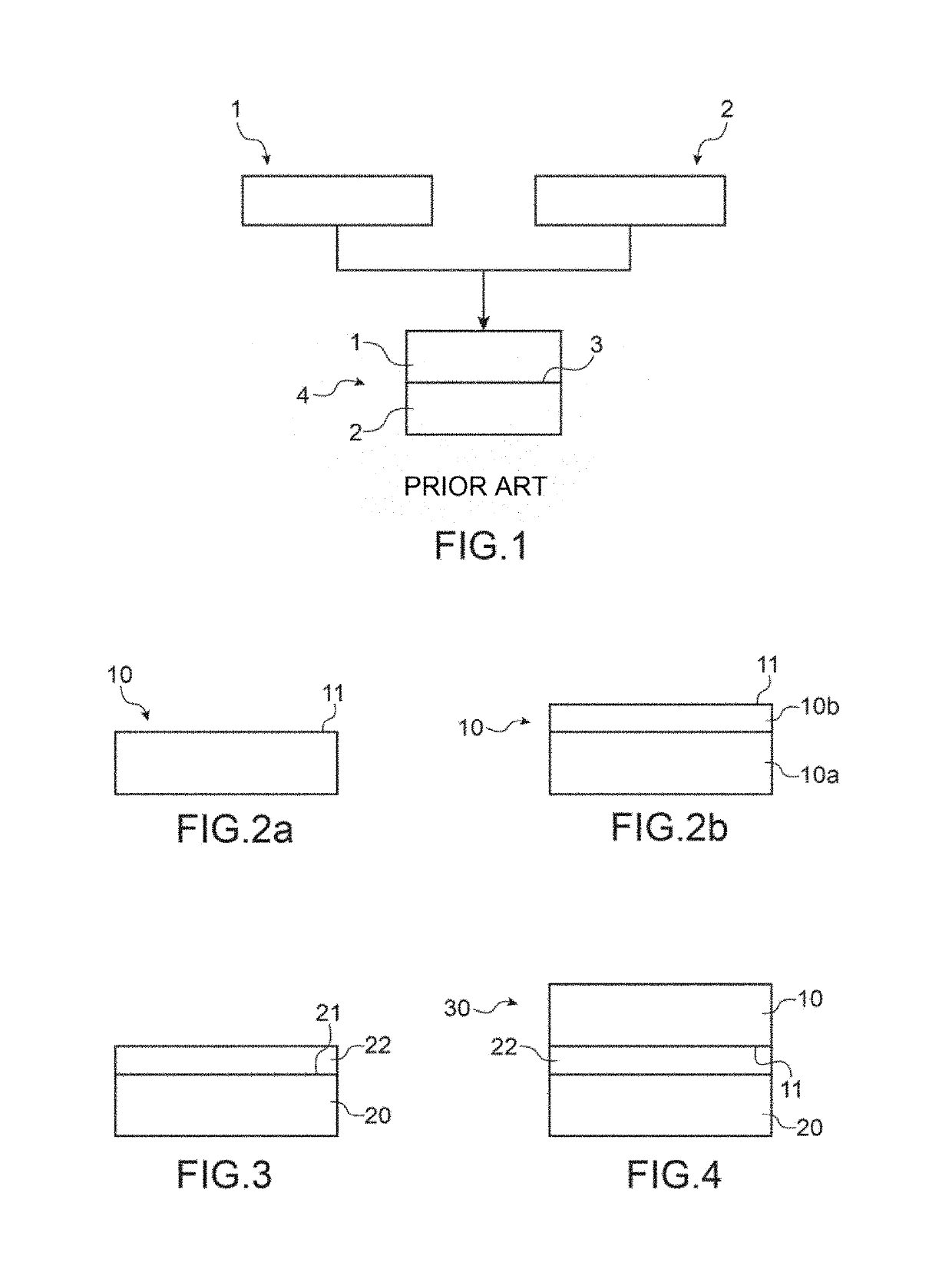
[0073] the method for assembling, shown in FIGS. 2a and 2b, comprises a step a) consisting in providing a first substrate 10.

[0074]The first substrate 10 comprises a first face 11.

[0075]The first face 11 is made from crystalline indium phosphide, advantageously the indium phosphide is monocrystalline.

[0076]Advantageously, the roughness of the first face 11 is suitable for direct bonding. For example, the roughness of the first face 11 is less than 1 nm RMS (“RMS” is the abbreviation of “Root Mean Square”), preferably less than 0.5 nm RMS, and very preferably less than 0.3 nm RMS, measured in 5 μm×5 μm atomic force microscopy scan.

[0077]The first substrate 10 can comprise a support substrate 10a whereon rests a layer of crystalline indium phosphide 10b. The exposed surface of the layer of crystalline indium phosphide 10b, advantageously monocrystalline, is then the first face 11.

[0078]The layer of indium phosphide 10b can have a thickness between 0.2 nm and 5 nm, preferably less than...

second embodiment

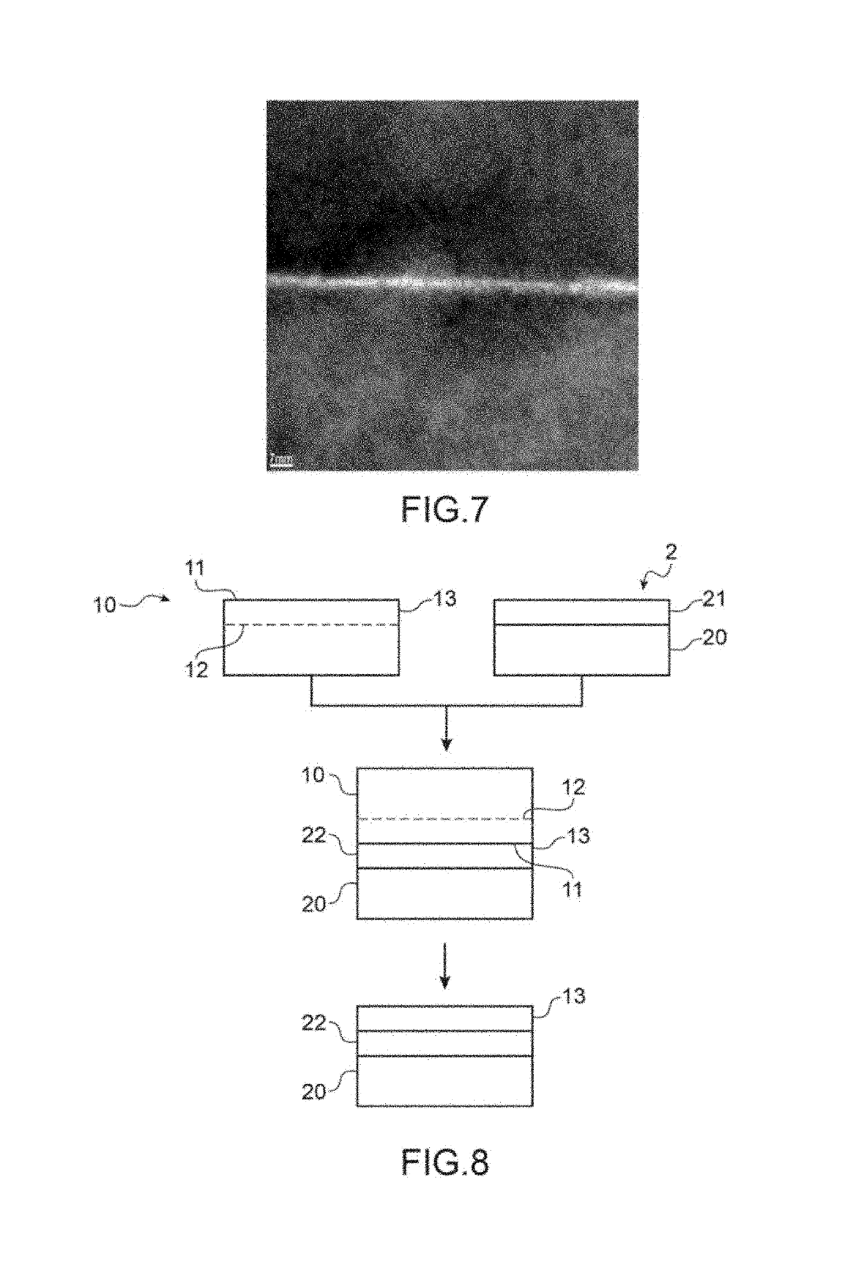
[0154]Still a step f) of fracture is executed after the step e) of assembling.

[0155]The step of fracturing comprises the initiation and the propagation of a fracture wave within the weakened area 12 in such a way that the first substrate 10 is detached from the useful layer 13, and as such allows for the transfer of said useful layer 13 on the exposed surface of the intermediate layer 22.

[0156]The step f) can be carried out by heat treatment, for example a treatment comprising an elevation in temperature.

[0157]Advantageously, the heat treatment is executed in an inert atmosphere, for example under Argon, at a temperature between 150° C. and 300° C., and a duration between 30 min and 3 h.

[0158]By way of example, for a dose of hydrogen of 6.5×10¹⁶ atm / cm2, implanted at an energy of 100 KeV in a first substrate 10 made of indium phosphide, an annealing executed at a temperature of 275° C., and a duration of 1 h 30 will allow for the initiation and the propagation of a fracture wave wi...


PUM

PropertyMeasurementUnit
roughnessaaaaaaaaaa
pressureaaaaaaaaaa
pressureaaaaaaaaaa

Abstract

The invention concerns an assembly method comprising the following steps: a) providing a first substrate comprising a first face made from crystalline indium phosphide, b) providing a second substrate comprising a second crystalline face different from the indium phosphide, c) forming an intermediate layer of crystalline indium phosphide on the second face of the second substrate, d) forming an assembly, via a direct bonding step, by bringing the first face of the first substrate into contact with the intermediate layer, the direct bonding step being carried out in an atmosphere having a pressure greater than 10−4 Pa, and preferably higher than 10−3 Pa, e) subjecting the assembly formed in step d) to heat treatment.

Description

TECHNICAL FIELD AND PRIOR ART[0001]The invention relates to a method for assembling a first substrate and a second substrate, the assembling being intended for use in the field of energy, optoelectronics, and microelectronics.[0002]FIG. 1 shows a method for assembling, known from prior art and described by Shiro Uchida et al. [1], that comprises the following steps:[0003]a) providing a first substrate 1 of crystalline indium phosphide comprising a first face,[0004]b) providing a second substrate 2 of crystalline gallium arsenide comprising a second face,[0005]c) executing a cleaning of the first face and of the second face,[0006]d) activating the first face and the second face with a bombardment by an argon ion beam,[0007]e) assembling the first face and the second face.[0008]At the end of the step e) of the known method of prior art, a heterostructure 4, comprising an assembly interface 3 between the first face and the second face, is obtained.[0009]The step c) of cleaning comprise...

Claims


Application Information

Patent Timeline
Patent Type & Authority Patents(United States)
IPC IPC(8): H01L21/46H01L21/18H01L23/00C09J5/06C09J5/02
CPCH01L21/187C09J5/02H01L24/83C09J5/06C09J2203/326H01L21/76254
Inventor IMBERT, BRUNOMORICEAU, HUBERTBLOT, XAVIER
Owner COMMISSARIAT A LENERGIE ATOMIQUE ET AUX ENERGIES ALTERNATIVES
Learn More