Super-fast wide-wave-band optical detector made by by doped oxide and silicon heterojunction material
A technology of silicon heterojunction and photodetector, which is applied in the field of high-sensitivity and anti-radiation photodetector, ultra-fast response, and wide frequency band, which can solve the problem of insufficient light response speed, insufficient sensitivity, and easy damage of the detector core and other issues, to achieve the effect of ultra-fast photoresponse, strong radiation resistance, and small capacitance
- Summary
- Abstract
- Description
- Claims
- Application Information
AI Technical Summary
Problems solved by technology
Method used
Image
Examples
Embodiment 1
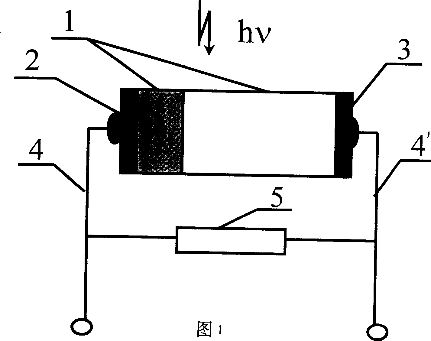
[0029] Referring to FIG. 1 , an optical sensor chip 1 is made of a doped lanthanum manganese oxide and a silicon heterojunction material, and an ultrafast wideband high-sensitivity optical detector is prepared.
[0030]In this embodiment, a substrate is an n-type silicon wafer, on which a 300nm-thick, p-type La 0.7 Sr 0.3 MnO 3 photoresponsive material layer, forming La 0.7 Sr 0.3 MnO 3 / Si two-layer heterogeneous material, cut the heterojunction material into a size of 1×0.2cm 2 The photosensor chip 1 of the photosensor chip 1; remove the silicon oxide on the silicon surface with hydrofluoric acid, weld the second electrode 3 of about φ2mm on the silicon surface of the photosensor chip 1 with indium, and use indium on the La of the photosensor chip 1 0.7 Sr 0.3 MnO 3 The surface of the film is welded with the first electrode 2; two φ0.1mm copper wires are used as electrode leads, and one end of the two φ0.1mm copper first electrode leads 4 and the second electrode lead...
Embodiment 2
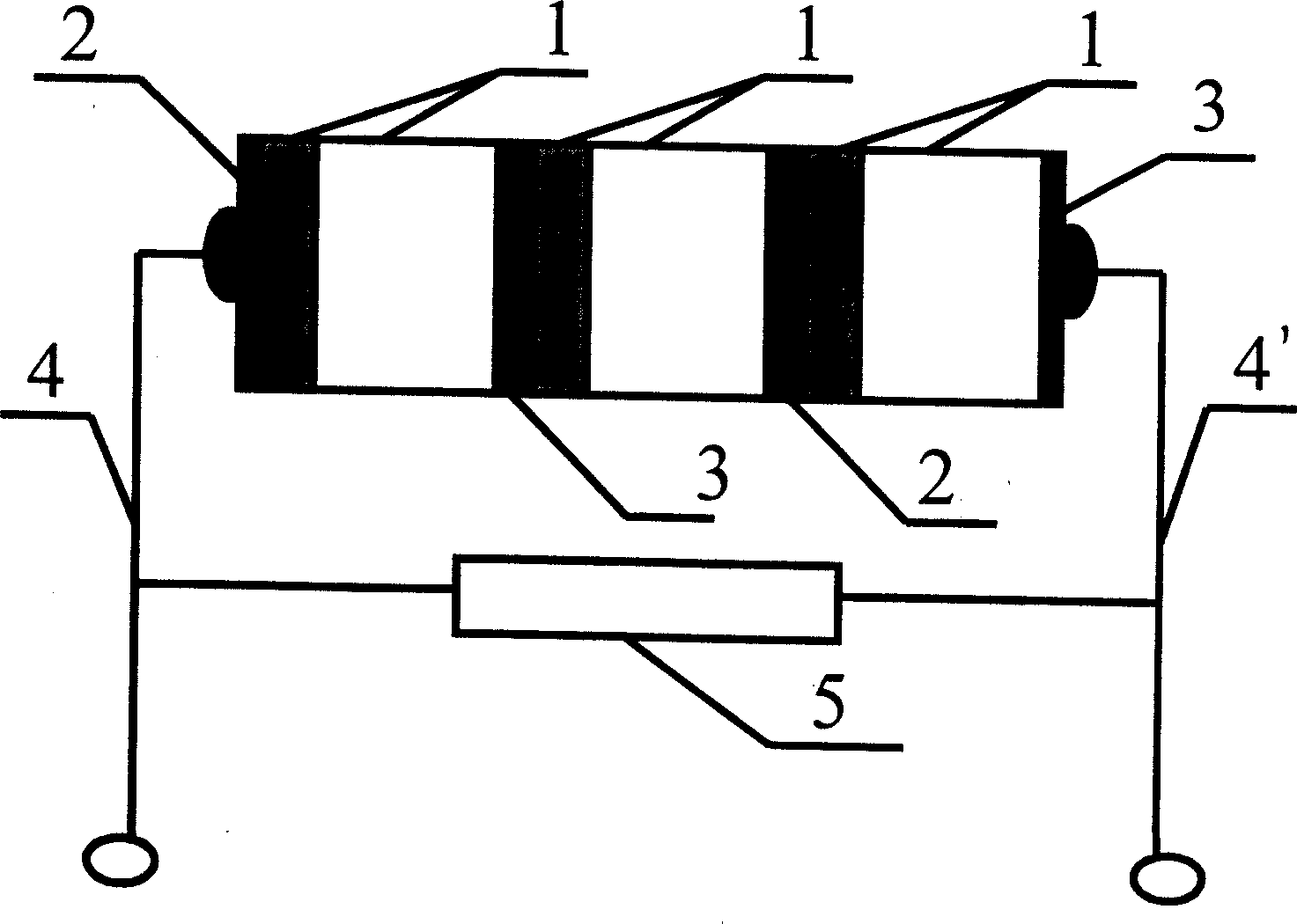
[0034] refer to figure 2 , select a 2-inch p-type silicon wafer, and directly epitaxially grow a 100nm-thick, n-type La on it 0.7 Te 0.3 MnO 3 To prepare heterojunction materials with thin films, after removing the oxide layer on the Si surface with FH, vacuum coating was used on La 0.7 Te 0.3 MnO 3 and Si surface by evaporation of silver film, the silver-coated La 0.7 Te 0.3 MnO 3 / Si two-layer heterogeneous material is cut into a rectangle of 10 mm × 2 mm as a detector chip, and the three detector chips are connected in series to make an optical sensor chip 1, wherein the La of the first detector chip is 0.7 Te 0.3 MnO 3 The surface of the thin film is in contact with the silicon substrate surface of the second photodetector chip and stacked, and so on, the La of the first photodetector chip after stacking 0.7 Te 0.3 MnO 3 The first electrode 2 of φ0.2mm copper wire is welded on the surface of the film; the second electrode 3 of φ2mm is welded on the silicon subs...
Embodiment 3
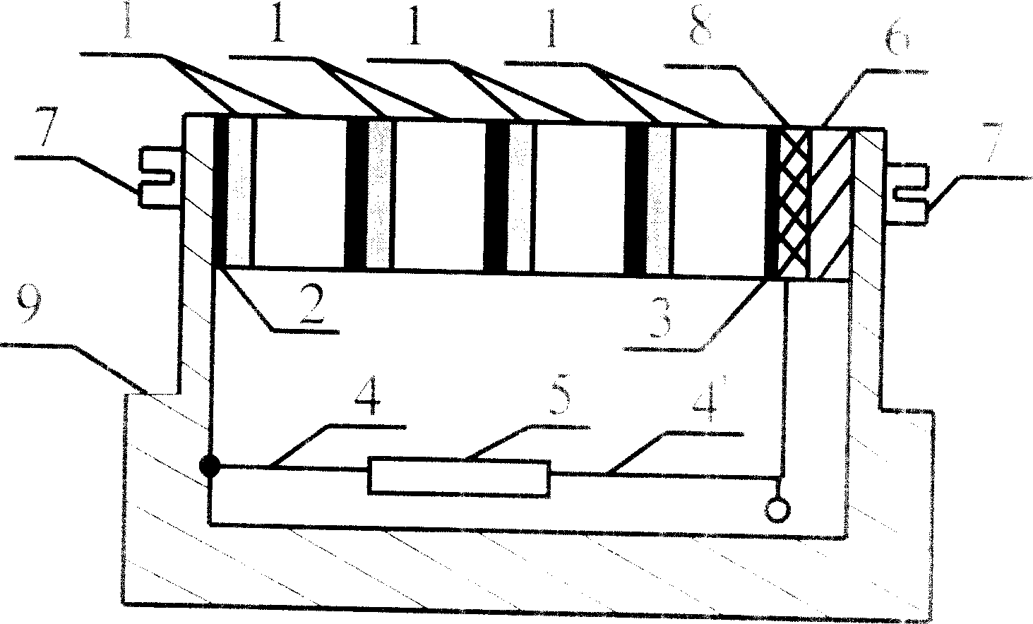
[0036] refer to image 3 , choose to make a layer of SrO buffer layer on the n-type silicon substrate, and then epitaxially grow 800nm thick La 0.95 Ba 0.05 MnO 3 Thin film, by vacuum coating method in La 0.95 Ba 0.05 MnO 3 Platinum thin film is plated on the surface of Si and Si respectively, and the La after plating platinum thin film 0.95 Ba 0.05 MnO 3 / Si heterojunction material is cut into 15mm×3mm rectangular blocks to make photodetector chips, and 8 pieces of 15mm×3mm La 0.95 Ba 0.05 MnO 3 / Si photodetector chips are connected in series to make photosensor chip 1, the La of the first photodetector chip 0.95 Ba 0.05 MnO 3 The surface of the film is laminated in contact with the silicon substrate of the second photodetector chip, and by analogy, the side of the laminated photosensor chip 1 is used as the incident surface of the detected light. The outermost La 0.95 Ba 0.05 MnO 3 The thin film serves as the first electrode 2 , and the outermost n-type sil...
PUM
 Abstract
Description
Claims
Application Information
 - R&D Engineer
- R&D Manager
- IP Professional
- Industry Leading Data Capabilities
- Powerful AI technology
- Patent DNA Extraction
Browse by: Latest US Patents, China's latest patents, Technical Efficacy Thesaurus, Application Domain, Technology Topic, Popular Technical Reports.
© 2024 PatSnap. All rights reserved.Legal|Privacy policy|Modern Slavery Act Transparency Statement|Sitemap|About US| Contact US: help@patsnap.com


