Nickel/piezoelectric ceramic laminar composite material with magnetoelectric effect and preparation process thereof
A technology of layered composite materials, magnetoelectric composite materials, applied in material selection for piezoelectric devices or electrostrictive devices, manufacture/assembly of magnetostrictive devices, manufacture/assembly of piezoelectric/electrostrictive devices and other directions, it can solve the problems of high material price, complex preparation process, small resistivity, etc., and achieve the effect of low price and simple preparation process
- Summary
- Abstract
- Description
- Claims
- Application Information
AI Technical Summary
Problems solved by technology
Method used
Image
Examples
Embodiment 1
[0019] Prepared by the following method figure 1 (a) The composite sample of the double-layer nickel / piezoelectric ceramic layer structure shown:
[0020] Step 1: A piezoelectric ceramic sheet 1 with a length of 30 mm, a width of 10 mm, and a thickness of 0.2 mm is plated with gold or silver electrodes on the upper and lower sides, and polarized along the thickness direction.
[0021] Step 2: A nickel sheet 2 with a length of 30 mm, a width of 10 mm, and a thickness of 0.1 mm was bonded to the piezoelectric ceramic sheet with a silver powder epoxy adhesive, and cured at room temperature to obtain a composite material sample with a double-layer structure.
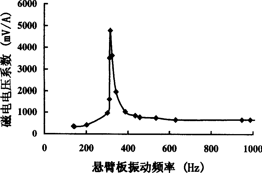
[0022] The experimental test curve of the magnetoelectric voltage coefficient dE / dH of the prepared composite material sample as a function of frequency is as follows figure 2 . The composite material reaches the maximum magnetoelectric voltage coefficient of 4.8V / A at the resonance frequency, and the magnetoelectric volt...
Embodiment 2
[0024] Prepared as follows figure 1 (b) The three-layer structure nickel / piezoelectric ceramic layered composite material sample:
[0025] Step 1: A piezoelectric ceramic sheet 1 with a length of 30 mm, a width of 10 mm, and a thickness of 0.2 mm is plated with gold or silver electrodes on the upper and lower sides, and polarized along the thickness direction.
[0026] Step 2: Use silver epoxy adhesive to bond two nickel sheets 2 with a length of 30 mm, a width of 10 mm, and a thickness of 0.1 mm to both sides of the piezoelectric ceramic sheet, and cure at room temperature to obtain a composite material with a three-layer structure sample.
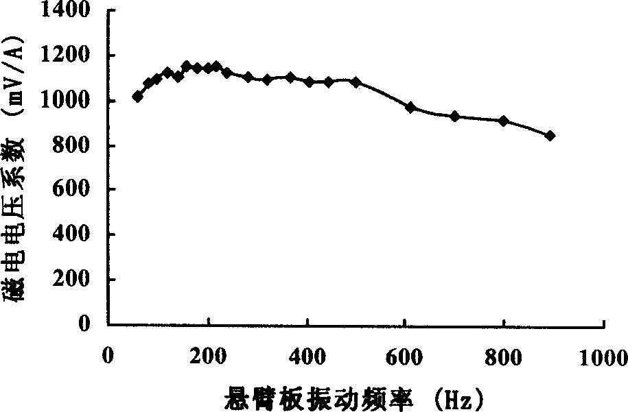
[0027] The experimental test curve of the magnetoelectric voltage coefficient dE / dH of the prepared composite material sample as a function of frequency is as follows image 3 shown. In the experimental test range, the magnetoelectric voltage coefficient of the three-layer structure composite material at the non-resonant frequency is 0.8...
Embodiment 3、4、5、6、7、8、9、10
[0029] Using the same bonding process as in Example 1 and Example 2, Ni sheets and piezoelectric ceramic sheets of different thicknesses are bonded together, then the magnetoelectric voltage coefficient of the layered composite material increases with the Ni sheet and piezoelectric ceramic sheet. The layer thickness ratio and lamination structure change, and the experimental results are shown in Table 1. The magnetoelectric voltage coefficient increases with the increase of Ni to piezoelectric ceramic layer thickness ratio. It should be noted that the resonant frequency of the three-layer board is very high. Due to the limitation of the test conditions, the experiment cannot measure the magnetoelectric voltage coefficient at the resonant frequency.
[0030]
[0031] 8
PUM
| Property | Measurement | Unit |
|---|---|---|
| Thickness | aaaaa | aaaaa |
| Length | aaaaa | aaaaa |
| Width | aaaaa | aaaaa |
Abstract
Description
Claims
Application Information
 - Generate Ideas
- Intellectual Property
- Life Sciences
- Materials
- Tech Scout
- Unparalleled Data Quality
- Higher Quality Content
- 60% Fewer Hallucinations
Browse by: Latest US Patents, China's latest patents, Technical Efficacy Thesaurus, Application Domain, Technology Topic, Popular Technical Reports.
© 2025 PatSnap. All rights reserved.Legal|Privacy policy|Modern Slavery Act Transparency Statement|Sitemap|About US| Contact US: help@patsnap.com


