
Method of machining semiconductor wafer-use polishing pad and semiconductor wafer-use polishing pad

A processing method, semiconductor technology, applied in semiconductor/solid-state device manufacturing, wheels with flexible working parts, metal processing equipment, etc., can solve problems such as large surface roughness and inability to form

Inactive Publication Date: 2005-03-09
JSR CORPORATIOON
View PDF2 Cites 8 Cited by
  • Summary
  • Abstract
  • Description
  • Claims
  • Application Information

AI Technical Summary

Problems solved by technology

However, even with the conventional polishing pad made of resin foam, it is not easy to perform fine cutting in the depth direction of the groove even if it is cut by the processing device as described above.
In addition, since the polishing pad is not so thick, it may not be possible to form ring-shaped or lattice-shaped grooves with high dimensional accuracy such as width and depth on the entire surface of the polishing pad.
Moreover, there is also the problem that the surface roughness of the inner surface of the groove on the polishing pad after cutting is relatively large.

Method used

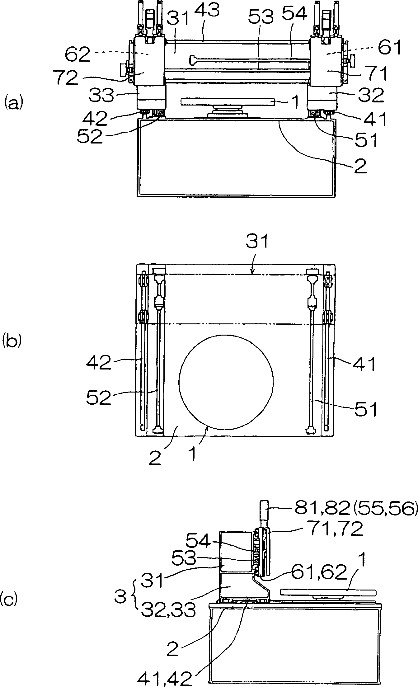
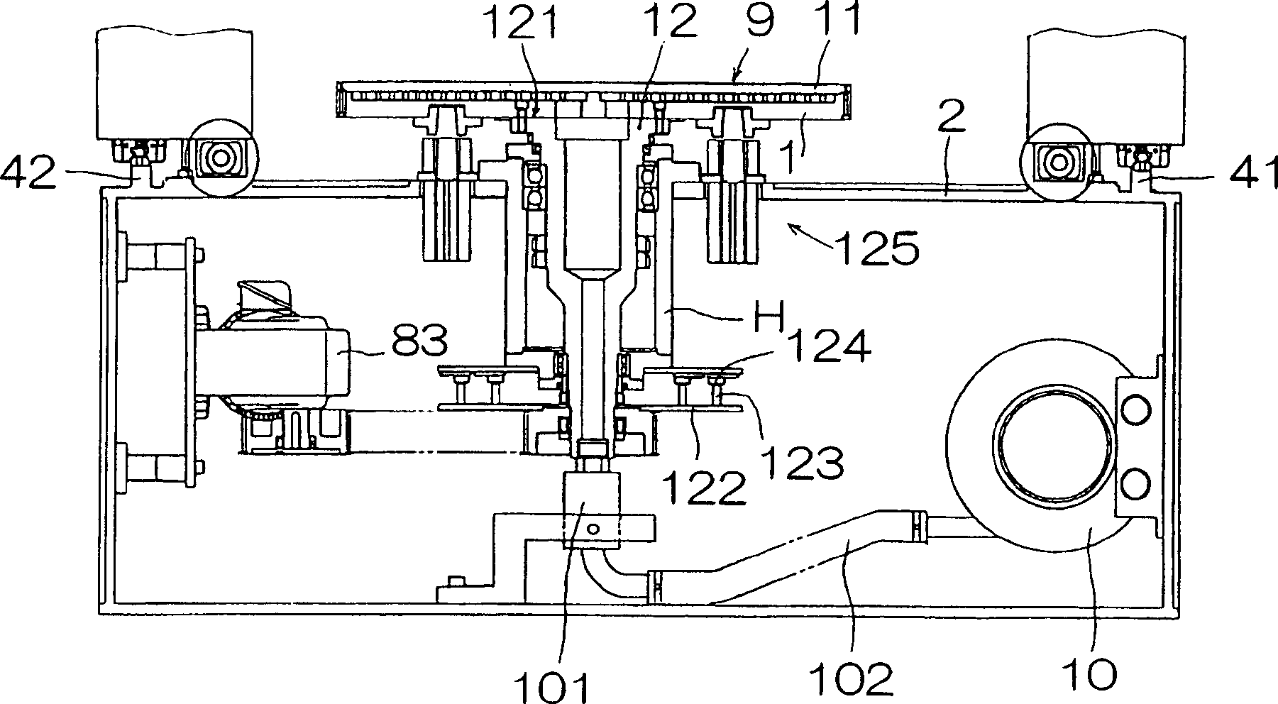
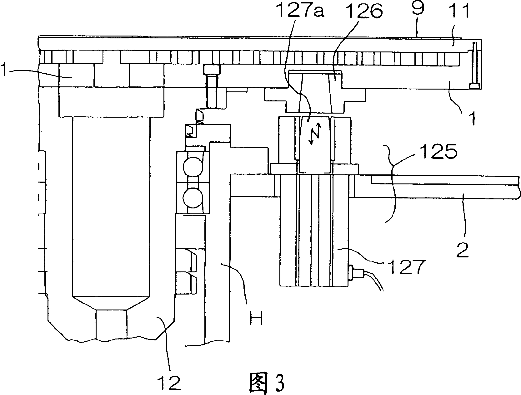

Image

  • Method of machining semiconductor wafer-use polishing pad and semiconductor wafer-use polishing pad
  • Method of machining semiconductor wafer-use polishing pad and semiconductor wafer-use polishing pad
  • Method of machining semiconductor wafer-use polishing pad and semiconductor wafer-use polishing pad

Examples


Embodiment 1

[0167] 70 parts by mass of uncrosslinked 1,2-polybutadiene (manufactured by JSR Corporation, product name "JSRRB830"), 30 parts by mass of uncrosslinked ethylene-vinyl acetate copolymer (manufactured by Tosoh Corporation, product name "Ultrathene 630") ”) and 40 parts by mass of β-cyclodextrin as water-soluble particles (manufactured by Yokohama International Bio Research Institute, product name “Dexipearl β-100”, average particle size: 20 μm) were extruded by biaxial extrusion at 160° C. machine for mixing. Thereafter, 1.0 parts by mass of an organic peroxide (manufactured by NOF Corporation, product name "Percumy D-40") was added to continue kneading, and the kneaded product was extruded into a metal mold, and then kept at 170° C. for 18 minutes, carry out cross-linking treatment, and obtain a polishing pad with a diameter of 60 cm and a thickness of 3 mm. Then, on the polishing surface side of the polishing pad, form a plurality of concentric annular grooves by the method ...

Embodiment 2

[0183] A polishing pad with the same size is manufactured in the same manner as in Example 1. On the polishing surface side of the polishing pad, a plurality of concentric annular grooves are formed by the method described in [2] above, wherein the groove width The average value of the groove depth is 0.5 mm, the average value of the groove depth is 1 mm, and the average value of the pitch is 1 mm.

[0184] The surface roughness of the inner surface of the groove was 5.2 μm, and the variation in surface roughness was also small. In addition, the dimensional accuracy is excellent, being ±4% in width, ±5% in depth, and ±5% in pitch. In addition, the polishing speed, the presence or absence of scratches, and the state of dishing were evaluated in the same manner as in Example 1. As a result, it was found that the polishing rate was 300 nm / min, scratches were hardly recognized, the dishing was 60 nm, and the flatness of the polished surface was excellent.

Embodiment 3

[0186] 80 parts by mass of uncrosslinked ethylene-vinyl acetate copolymer (manufactured by Tosoh Corporation, product name "Ultrathene 630"), 20 parts by mass of uncrosslinked 1,2-polybutadiene (manufactured by JSR Corporation, product name "JSR RB830") and 100 parts by mass of β-cyclodextrin as water-soluble particles (manufactured by Yokohama International Bio Research Institute, product name "Dexipearl β-100", average particle size: 20 μm) were extruded by a biaxial extrusion machine with a temperature adjusted to 160°C. Exit the machine for mixing. Thereafter, 0.5 parts by mass of an organic peroxide (manufactured by NOF Corporation, product name "Percumyl D-40") was added, kneading was continued, and the kneaded product was extruded into a mold whose temperature was adjusted to 170°C. Thereafter, it was directly kept at 170° C. for 18 minutes to carry out cross-linking treatment to obtain a polishing pad with a diameter of 60 cm and a thickness of 3 mm. Then, on the poli...


PUM

PropertyMeasurementUnit
surface roughnessaaaaaaaaaa
angleaaaaaaaaaa
particle sizeaaaaaaaaaa

Abstract

An object of the invention is to provide a processing method of a polishing pad for semiconductor wafer capable of forming a groove, a concave portion, a through hole and the like having a small surface roughness of the inner surface of the groove and the like of 20 mu m or less, a high dimensional accuracy and a uniform cross-sectional shape, and a polishing pad for semiconductor wafer. In the present processing method, a surface of a polishing pad comprising a water-insoluble matrix containing a crosslinked polymer and a water-soluble particle dispersed in the water-insoluble matrix is processed by cutting and the like. Additionally, when a groove and the like are formed, it is preferable that a polishing pad is placed on one surface side of a machining table having a sucking hole, the pad is fixed on the one surface side of the machining table by vacuuming sucking it from the other surface of the machining table, and then a groove and the like are formed.

Description

technical field [0001] The present invention relates to a processing method of a polishing pad for semiconductor wafers and a polishing pad for semiconductor wafers in which grooves, recesses, through holes, etc. are formed on the polishing surface of the polishing pad by the method. More specifically, it relates to a method of processing a semiconductor wafer polishing pad for forming annular grooves, lattice grooves, spiral grooves, a plurality of recesses, through holes, and the like on a polishing surface. The polishing pad for semiconductor wafers produced by this method is used for the chemical mechanical polishing (Chemical Mechanical Polishing) (henceforth "CMP") of a semiconductor wafer etc.. Background technique [0002] Polishing pads made of resin are often used in CMP processing of semiconductor wafers. In order to hold the slurry for CMP, temporarily store polishing shavings, etc., ring-shaped grooves, lattice-shaped grooves, spiral grooves, etc. are sometimes...

Claims


Application Information

Patent Timeline
Patent Type & Authority Applications(China)
IPC IPC(8): B23K26/08B23K26/36B23K26/38B24B37/24B24B37/26B24D13/14B24D18/00C09C1/68
CPCB23K26/367B23K26/0807B23K26/403B23K26/407B24B37/26B23K26/381B24D18/00B23K26/0823B23K26/4075B23K26/4065B24B37/24B23K2203/10B23K26/402B23K26/40B23K26/082B23K26/364B23K26/382B23K2103/30B23K2103/42B23K2103/50H01L21/304
Inventor 志保浩司长谷川亨川桥信夫
Owner JSR CORPORATIOON
Learn More