Method for constituting graph on intermetallic dielectric layer
A technology for intermetallic dielectric layers and dielectric layers, which is applied in the manufacture of circuits, electrical components, semiconductors/solid-state devices, etc., and can solve problems such as increasing the dielectric constant of low dielectric layers and reducing the reliability of low dielectric layers
- Summary
- Abstract
- Description
- Claims
- Application Information
AI Technical Summary
Problems solved by technology
Method used
Image
Examples
Embodiment 1
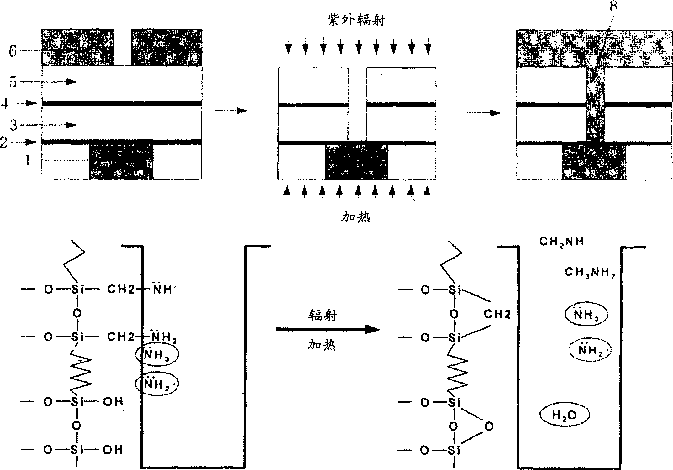
[0023] The present invention can be better understood through the following examples, which are illustrative and should not be construed as limiting the present invention. Example 1: Comparison of the chemical composition of the inner walls of the vias before and after UV radiation
[0024] Due to the difficulty in analyzing the chemical composition constituting the inner wall of the small-sized via hole, a dielectric layer (a non-porous SiOC layer) was placed on the semiconductor substrate, and the N 2 Dry etching without a photoresist pattern was performed under an atmosphere, and then the chemical composition constituting the surface of the SiOC layer was analyzed using TOF-SIMS as the chemical composition of the via hole. The results are listed in Figure 4 . from Figure 4 It can be seen that only hydrocarbons were found after placement of the dielectric layer, but a large amount of carbonitride and nitrogen-containing amino species were found after the dry etching pr...
Embodiment 2
[0027] Example 2: Formation of via holes
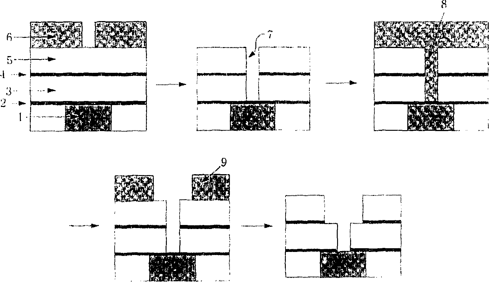
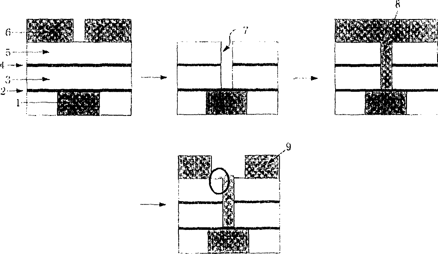
[0028] A lower circuit is formed on the semiconductor substrate, and a lower etch stop layer, a lower dielectric layer, an upper etch stop layer and an upper dielectric layer are sequentially disposed on the lower circuit. At this time, non-porous silicon carbide (SiC) layers and SiOC layers are used as upper and lower etch stop layers and upper and lower dielectric layers, respectively. Then photoresist is coated on the upper and lower dielectric layers, exposed and developed to form a photoresist pattern. Use the photoresist pattern as a mask to dry etch the upper dielectric layer, the upper etch-stop layer and the lower dielectric layer in sequence to expose the lower etch stop layer 2 on the lower circuit, thereby forming a via hole in the dielectric layer .
[0029] Using a mercury lamp light source to irradiate the via hole with ultraviolet light for 60 seconds while heating at 200°C to remove the etching residue on the inner ...
PUM
| Property | Measurement | Unit |
|---|---|---|
| Wavelength | aaaaa | aaaaa |
Abstract
Description
Claims
Application Information
 - R&D Engineer
- R&D Manager
- IP Professional
- Industry Leading Data Capabilities
- Powerful AI technology
- Patent DNA Extraction
Browse by: Latest US Patents, China's latest patents, Technical Efficacy Thesaurus, Application Domain, Technology Topic, Popular Technical Reports.
© 2024 PatSnap. All rights reserved.Legal|Privacy policy|Modern Slavery Act Transparency Statement|Sitemap|About US| Contact US: help@patsnap.com


