
High-temperature superconductive coating conductor dual-layer buffering layer structure and dynamic deposition method thereof

A technology of coated conductors and high-temperature superconductors, applied in superconducting/high-conducting conductors, usage of superconducting elements, coatings, etc., can solve problems such as increasing costs, and achieve diffusion prevention, chemical stability and good structural matching , the effect of uniform texture orientation

Active Publication Date: 2014-07-30
SHANGHAI UNIV
View PDF7 Cites 0 Cited by
  • Summary
  • Abstract
  • Description
  • Claims
  • Application Information

AI Technical Summary

Problems solved by technology

At present, although these three structures can meet the epitaxial growth of the final superconducting layer, the complex three-layer structure increases the cost of the deposition process and batch preparation

Method used


Image

  • High-temperature superconductive coating conductor dual-layer buffering layer structure and dynamic deposition method thereof
  • High-temperature superconductive coating conductor dual-layer buffering layer structure and dynamic deposition method thereof
  • High-temperature superconductive coating conductor dual-layer buffering layer structure and dynamic deposition method thereof

Examples


Embodiment 1

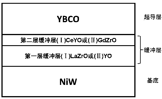
[0039] Preparation of La by Reactive Magnetron Sputtering 2 Zr 2 o 7 / C 2 Y 2 o 7 Double buffer layer structure.

[0040] A. Ce for sputtering 2 Y 2 o 7 The target material adopts Ce and Y alloy metal targets with an atomic number of 1:1, and La for sputtering 2 Zr 2 o 7 The target is spliced ​​with two semicircles, half of which are La and half Zr. The purity of metal targets and alloy targets is greater than 99.9%.

[0041] B. Pretreatment of the metallic NiW substrate before performing the entire deposition process. at a temperature of 700°C and ArH 2 Carry out heat treatment to metal substrate in the atmosphere, the time of heat treatment is 40 minutes, wherein ArH 2 H in 2 The proportion of the medium is 5%, and the overall air pressure is maintained at 1Pa.

[0042] C. Use the LaZr alloy target first, and before the entire deposition process, vacuum the cavity to 10 -5 Below Pa, then pass Ar5%H into the cavity 2 , the flow rate of the mass flow meter is...

Embodiment 2

[0048] Embodiment 2 utilizes reactive magnetron sputtering to prepare Y 2 o 3 / Gd 2 Zr 2 o 7 Double buffer layer structure.

[0049] A. Gd for sputtering 2 Zr 2 o 7 The target material adopts Gd and Zr alloy metal targets with atomic numbers of 1:1, and the Y for sputtering 2 o 3 The target material is Y metal target, and the purity of metal target material and alloy target material is greater than 99.9%.

[0050] B. The metallic NiW substrate is pretreated before performing the entire deposition process. at a temperature of 700°C and ArH 2 Carry out heat treatment to metal substrate in the atmosphere, the time of heat treatment is 40 minutes, wherein ArH 2 H in 2 The proportion of the medium is 5%, and the overall air pressure is maintained at 1Pa.

[0051] C. Use the Y target first, and before the entire deposition process, evacuate the cavity to less than 10 -5 Below Pa, then pass Ar5%H into the cavity 2 , the flow rate of the mass flowmeter is 350 SCCM, and ...


PUM

PropertyMeasurementUnit
thicknessaaaaaaaaaa
thicknessaaaaaaaaaa

Abstract

The invention relates to a high-temperature superconducting coating conductor double-layer buffer layer structure and a dynamic deposition method thereof. Simplified double-layer rare earth oxide buffer layer structures, including (I) La2Zr2O7 / Ce2Y2O7 and (II) Y2O3 / La2Zr2O7, were epitaxially grown on Ni-5%W substrates with biaxial texture orientation by reactive sputtering. That is, the first buffer layer (lower buffer layer) and the second buffer layer (upper buffer layer) form a high-temperature superconducting coating conductor double-layer buffer layer structure. The metallic NiW substrate was pretreated before the reactive sputter deposition process. Carry out heat treatment on the metal substrate at a temperature of 700°C and in an ArH2 atmosphere; vacuum the back of the cavity to below 10-5Pa; inject water vapor during sputtering, and control the water pressure at 2.1×10⁻²Pa; the total pressure of the entire cavity Control at 1Pa; temperature at 800°C; after full pre-sputtering, power control at 160W. Sputtering deposition first deposits the first layer and then deposits the second layer. Finally, a double-layer rare earth oxide buffer layer is obtained.

Description

technical field [0001] The invention relates to a preparation method of a high-temperature superconducting coating conductor double-layer buffer layer structure, which belongs to the technical field of superconducting materials. Background technique [0002] The high-temperature superconducting coated conductor developed based on biaxial texture and thin-film epitaxy technology has a very good performance in the liquid nitrogen temperature region due to the large number of dislocation pinning centers generated by overcoming the weak connection between grain boundaries and the island growth mechanism. High critical current density and irreversible field. It breaks through the limitations of the first-generation Bi-based materials that are only suitable for direct current and low temperature, and makes it possible for the wide application of high-temperature superconductivity in power engineering, so it has become a research hotspot for practical superconducting materials. ...

Claims


Application Information

Patent Timeline
Patent Type & Authority Patents(China)
IPC IPC(8): H01B12/00H01B13/00C23C14/34C23C14/06C23C14/08
CPCY02E40/64Y02E40/60
Inventor 蔡传兵范峰赵荣鲁玉明刘志勇
Owner SHANGHAI UNIV
Learn More