Method for preparing nano CMOS parts by using side wall and solid phase diffusion of polysilicon

A technology of polysilicon and sidewalls, applied in semiconductor/solid-state device manufacturing, electrical components, circuits, etc., can solve problems such as high surface impurity concentration, high impurity activation rate, high temperature, etc., achieve the effect of reducing requirements and overcoming technical difficulties

Inactive Publication Date: 2003-05-07
SEMICON MFG INT (SHANGHAI) CORP +1
View PDF0 Cites 6 Cited by
  • Summary
  • Abstract
  • Description
  • Claims
  • Application Information

AI Technical Summary

Problems solved by technology

Solid phase diffusion can achieve relatively high surface impurity concentration and high impurity activation rate. The main disadvantage is that solid phase diffusion requires relatively high temperature (usually >1000°C), and the uniformity and repeatability of the process need to be improved.
PSG, BSG, etc. can only realize one kind of transistor and cannot realize CMOS at the same time, so CMOS circuits cannot be realized; the low-energy ion implantation SiO2+ solid phase diffusion process is relatively complicated, and ultra-low energy ion implantation is also required; polysilicon is widely used in MOS technology It is used as a solid-phase diffusion source for P+N junctions to realize PMOS transistors. At present, there are no reports for simultaneous realization of P+N and N+P ultra-shallow junctions.

Method used


Image

  • Method for preparing nano CMOS parts by using side wall and solid phase diffusion of polysilicon
  • Method for preparing nano CMOS parts by using side wall and solid phase diffusion of polysilicon
  • Method for preparing nano CMOS parts by using side wall and solid phase diffusion of polysilicon

Examples


Embodiment Construction

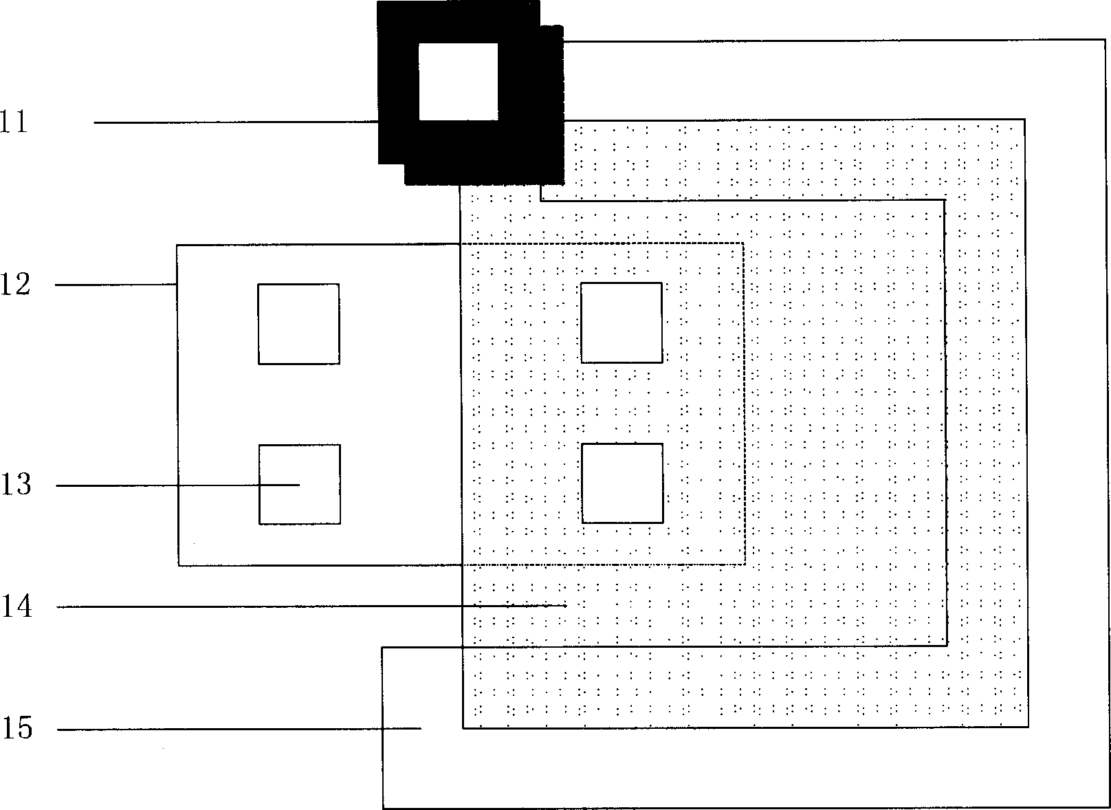
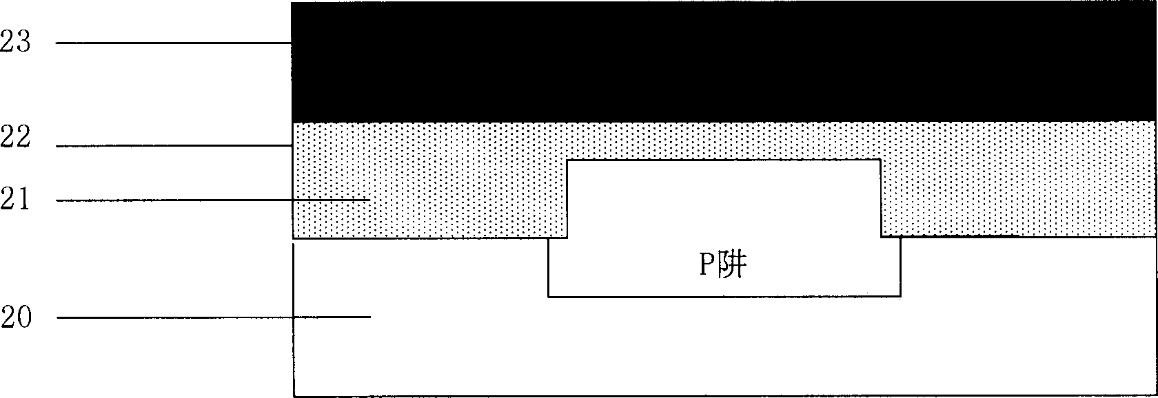
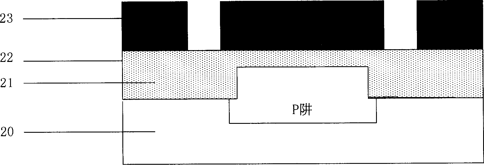
[0052] The method of the present invention is fully compatible with the traditional bulk silicon double-well CMOS process, uses sidewall transfer to make gate lines and heavily doped polysilicon as a diffusion source to form an ultra-shallow junction in the source and drain regions, and organically combines the two to finally realize Nanoscale CMOS transistors and devices. The following are specific examples.

[0053] A bulk silicon P(100) silicon wafer is used, and the resistivity of the substrate 20 is 10-15Ω·cm. Of course, an SOI chip can also be used, the difference is that no well needs to be fabricated.

[0054] 1. Using double well technology, two-step well pushing method: first, photolithography N well, and then implanting phosphorus into the well, 80~120Kev, 1.0~4.0E13cm -2 , then at 1000°C, hydrogen-oxygen synthesis and oxidation of about 150-200nm silicon dioxide, and N-well advancement at the same time; followed by photolithography in the P-well area, and well im...


PUM


Abstract

The invention relates to the technique area for manufacturing very large integrated circuit, including following steps. (1) Designing the pattern of the cell. (2) Insulating components, oxidizing grids and depositing the polysilicon of the grids, before this step, the trap is made based on the need. (3) The lines of the grids are made by using the side wall translocation (4) Depositing silicon dioxide, then reactive ion etching silicon dioxide forms the side wall. Complement area of CMOS LDD is prepared by polysilicon solid diffusion. (5) Depositing silicon dioxide, reactive ion etching silicon dioxide forms, the side wall of the final components. (6) The general following up procedures form the source and the drain electrodes. Etching the contact hole, forming the metal line to connect components.

Description

Technical field: [0001] The invention relates to a method for preparing nanometer CMOS devices and circuits in the technical field of ultra-large-scale integrated circuits (ULSI), especially using sidewall transfer to realize gate lines of nanoscale MOS transistors and using heavily doped polysilicon as a solid-phase diffusion source to realize CMOS LDD regions Ultra-shallow junctions, and thus methods for the eventual realization of nanoscale CMOS devices and circuits. Background technique: [0002] As the size of the device shrinks, its characteristic physical dimensions such as channel length, PN junction depth in source and drain regions, and gate dielectric thickness are also scaled down. It is more difficult to make nanoscale gate lines and shallower LDD region PN junctions (≤50nm). , becoming the most difficult areas in the IC development process. [0003] At present, the fabrication methods of nanoscale fine grid lines mainly include traditional lithography technolo...

Claims


Application Information

Patent Timeline
Patent Type & Authority Applications(China)
IPC IPC(8): H01L21/8238
Inventor 刘文安刘金华黄如张兴
Owner SEMICON MFG INT (SHANGHAI) CORP
Why Eureka
Try Eureka