Carbon doped silicon sheet with internal impurity absorbing function and production thereof
A carbon-silicon wafer and functional technology, applied in the field of carbon-doped silicon wafer preparation, can solve the problem of low micro-defect density, achieve good gettering effect, high internal gettering capacity, and improve yield
- Summary
- Abstract
- Description
- Claims
- Application Information
AI Technical Summary
Problems solved by technology
Method used
Image
Examples
Embodiment 1
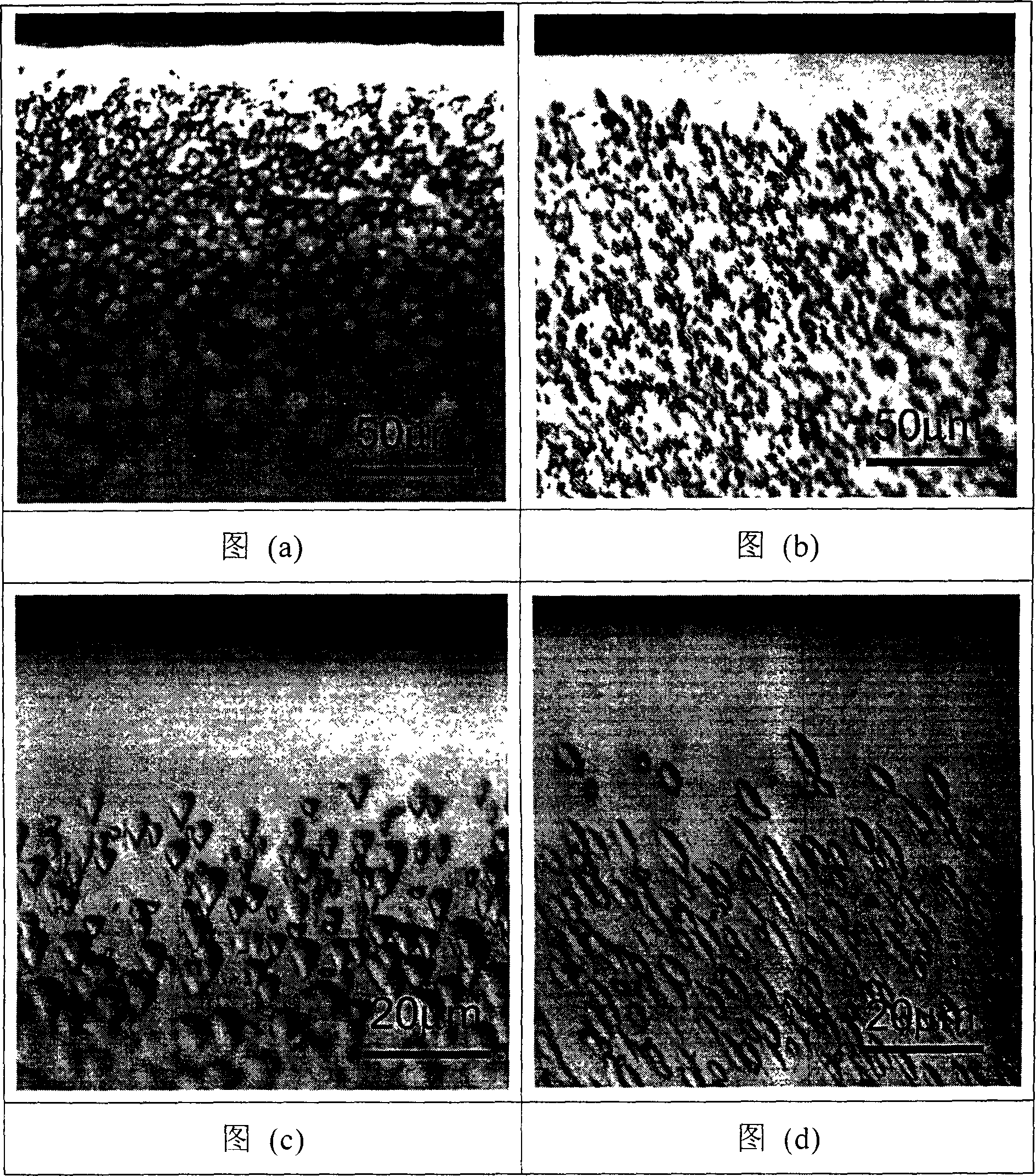
[0014] Select a 3-inch carbon-doped Czochralski silicon wafer (HCCZ-Si) grown under the protection of argon, with a carbon concentration of 1×10 17 cm -3 , the oxygen concentration is 8×10 17 cm -3 , The resistivity is 10 ohms. cm. In order to form a clean area and a bulk defect area in the silicon wafer, the silicon wafer is kept in a heat treatment furnace at 1200°C for 2 hours, then at 750°C for 16 hours, and after the treatment is completed at 1050°C for 16 hours. All heat treatments were performed under an argon atmosphere. After heat treatment, the silicon wafer was cleaved and etched in Sirtl preferential etching solution for 5 minutes, and then the distribution of defects on the cleavage plane was observed and photographed with an OLYMPUS MX50 microscope.
[0015] For comparison, an ordinary Czochralski silicon single crystal (CZ-Si) with the same oxygen concentration and resistivity, and a carbon concentration below the infrared detection limit, was also subjected...
Embodiment 2
[0018] Choose a 3-inch carbon-doped Czochralski silicon wafer grown under the protection of argon, with a carbon concentration of 5×10 16 cm -3 , the oxygen concentration is 15×10 17 cm -3 , The resistivity is 1 ohm. cm. Put the silicon wafer into the heat treatment furnace at 1150°C and keep it warm for 2 hours, then keep it at 650°C for 50 hours, and keep it at 1100°C for 6 hours after the treatment. All heat treatments were performed under an argon atmosphere. A silicon wafer with internal gettering ability can be obtained, with a certain width of defect-free clean area near the surface and a certain density of micro-defects (oxygen precipitation and secondary defects) in the body.
Embodiment 3
[0020] Select a 4-inch carbon-doped Czochralski silicon wafer grown under the protection of argon, with a carbon concentration of 3×10 17 cm -3 , the oxygen concentration is 6×10 17 cm -3 , The resistivity is 20 ohms. cm. Put the silicon wafer into the heat treatment furnace at 1250°C and keep it warm for 0.5 hours, then keep it at 850°C for 10 hours, and keep it at 1200°C for 20 hours after the treatment. All heat treatments were performed under an argon atmosphere. It is also possible to obtain a silicon wafer with internal gettering ability, a clean area with a certain width and no defects near the surface, and a certain density of micro-defects (oxygen precipitation and secondary defects) in the body.
PUM
 Abstract
Description
Claims
Application Information
 - R&D
- Intellectual Property
- Life Sciences
- Materials
- Tech Scout
- Unparalleled Data Quality
- Higher Quality Content
- 60% Fewer Hallucinations
Browse by: Latest US Patents, China's latest patents, Technical Efficacy Thesaurus, Application Domain, Technology Topic, Popular Technical Reports.
© 2025 PatSnap. All rights reserved.Legal|Privacy policy|Modern Slavery Act Transparency Statement|Sitemap|About US| Contact US: help@patsnap.com

