Etching method for opening with high height-to-width ratio

An etching and high-tech technology, which is applied in the fields of electrical components, semiconductor/solid-state device manufacturing, circuits, etc., can solve problems such as inability to further etch, unclean etching, process failure, etc.

Inactive Publication Date: 2005-06-15
WINBOND ELECTRONICS CORP
View PDF0 Cites 0 Cited by
  • Summary
  • Abstract
  • Description
  • Claims
  • Application Information

AI Technical Summary

Problems solved by technology

Once the etching process of the deep trench hole hard mask is stopped, further etching will not be possible, resulting in unclean etching, which will lead to the failure of the subsequent process and greatly reduce the yield of the semiconductor process.
Therefore, in the semiconductor manufacturing process where the process margin is shrinking, it is difficult to increase the aspect ratio of the hole while maintaining the etching margin.

Method used


Image

  • Etching method for opening with high height-to-width ratio
  • Etching method for opening with high height-to-width ratio
  • Etching method for opening with high height-to-width ratio

Examples


Embodiment Construction

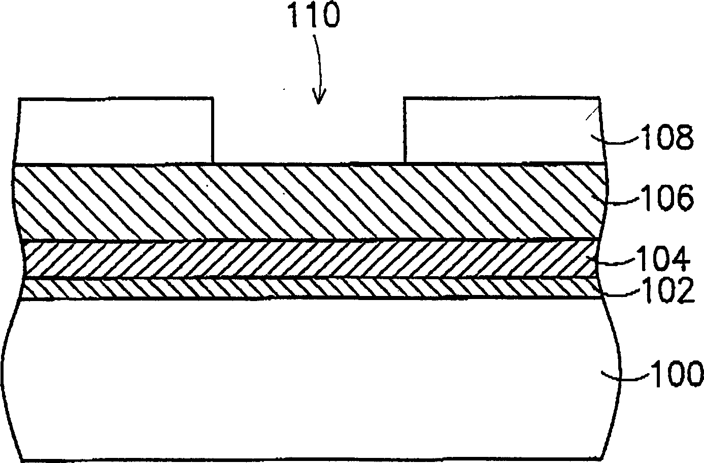
[0024] Please refer to figure 1 , forming a silicon oxide layer 102 on the substrate 100, the method for forming the silicon oxide layer 102 includes chemical vapor deposition or thermal oxidation. A silicon nitride layer 104 is formed on the silicon oxide layer 102, and the method for forming the silicon nitride layer 104 includes chemical vapor deposition. A silicon oxide layer 106 is formed on the silicon nitride layer 104, and the method for forming the silicon oxide layer 102 includes chemical vapor deposition. A layer of photoresist is coated on the silicon oxide layer 106 , and the layer of photoresist is patterned by a known lithography process to form a patterned photoresist layer 108 . The photoresist layer 108 includes a photoresist opening 110 , and the photoresist opening 110 exposes a portion of the silicon oxide layer 106 under the photoresist layer 108 .

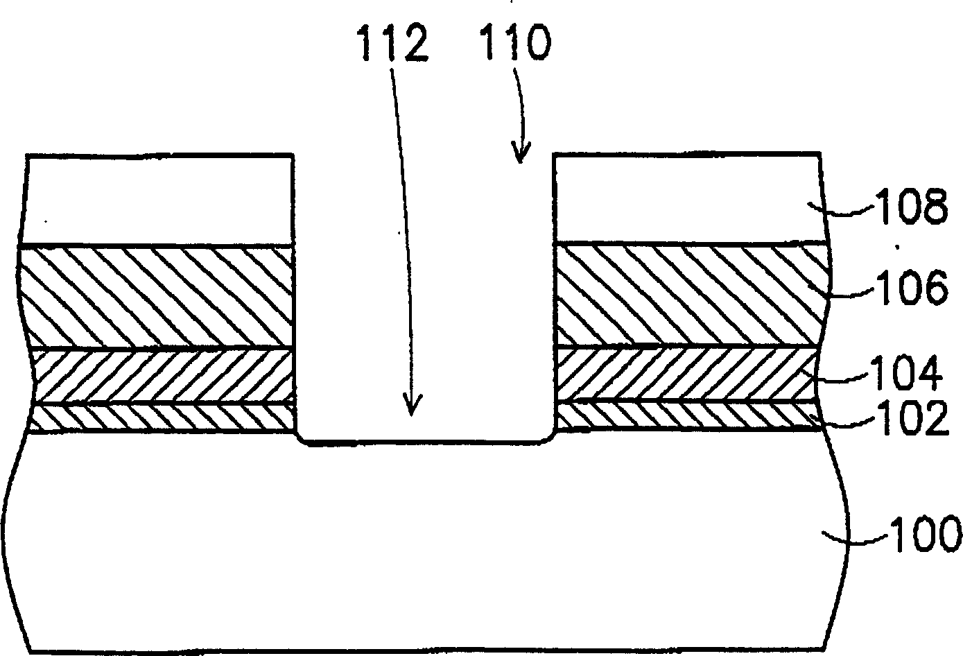
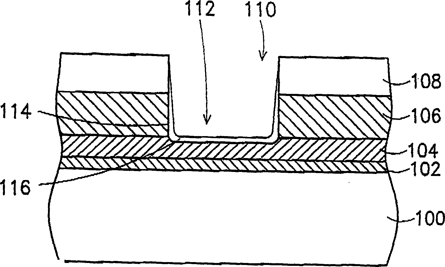
[0025] Please refer to figure 2 , using the photoresist layer 108 as a mask, the exposed part of the s...


PUM


Abstract

The invention relates to an etching method of a high aspect ratio opening, the etching method comprises: forming an opening by anisotropically etching the layer to be etched to be etched with a plasma etching condition having a polymer reaction, and the polymer reaction will A polymer film is formed on the sidewall of the opening and the bottom of the opening. This polymer film will slow down the plasma etching rate or even stop the etching. The polymer at the bottom of the opening is etched non-uniformly by another plasma etching condition. until the polymer film located at the bottom of the opening is completely stripped off, and then continue to anisotropically etch the material layer under the original plasma etching conditions until the etching of the opening is completed. The invention can effectively prevent the occurrence of the situation of stopping etching, and there will be no phenomenon of unclean etching.

Description

technical field [0001] The present invention relates to an etching method for forming a High Aspect Ratio opening (Opening), in particular to an etching method for avoiding the etching stop caused by the polymer film generated during etching. Background technique [0002] In the early semiconductor manufacturing process, the aspect ratio of the contact window was not high due to the low requirement on the degree of integration. With the development of semiconductor technology, in the advanced Very Large Scale Integration (VLSI) manufacturing process, the requirement for integration is getting higher and higher, thus resulting in higher aspect ratio of the contact window. When the semiconductor manufacturing process has entered the era of nanometers, since the size of semiconductor components is getting smaller and smaller, the aspect ratio of the openings to be formed in the components is getting higher and higher, and the difficulty of etching technology is also relatively ...

Claims


Application Information

Patent Timeline
Patent Type & Authority Patents(China)
IPC IPC(8): H01L21/306H01L21/3065
Inventor 周全启
Owner WINBOND ELECTRONICS CORP
Why Eureka
Try Eureka