Texture baffle capable of reducing semiconductor coating stress residue

A semiconductor and texture technology, applied in sputtering coating, vacuum evaporation coating, ion implantation coating, etc., can solve problems such as peeling, increase surface adhesion thickness, surface stress residual, etc., to reduce design cost, switching and testing Convenient and fast, reducing the effect of stress residual

Pending Publication Date: 2022-07-15
重庆臻宝实业有限公司
View PDF0 Cites 0 Cited by
  • Summary
  • Abstract
  • Description
  • Claims
  • Application Information

AI Technical Summary

Problems solved by technology

The existing technology is to increase the surface area by sandblasting and spraying, thereby increasing the surface adhesion thickness. This irregular or uneven surface morphology will exist in the residual surface stress. Excessive stress residue after surface coating is easy to cause peeling and turtles. crack phenomenon

Method used


Image

  • Texture baffle capable of reducing semiconductor coating stress residue
  • Texture baffle capable of reducing semiconductor coating stress residue
  • Texture baffle capable of reducing semiconductor coating stress residue

Examples


Embodiment Construction

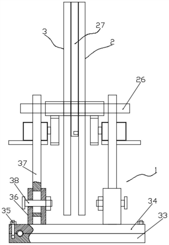
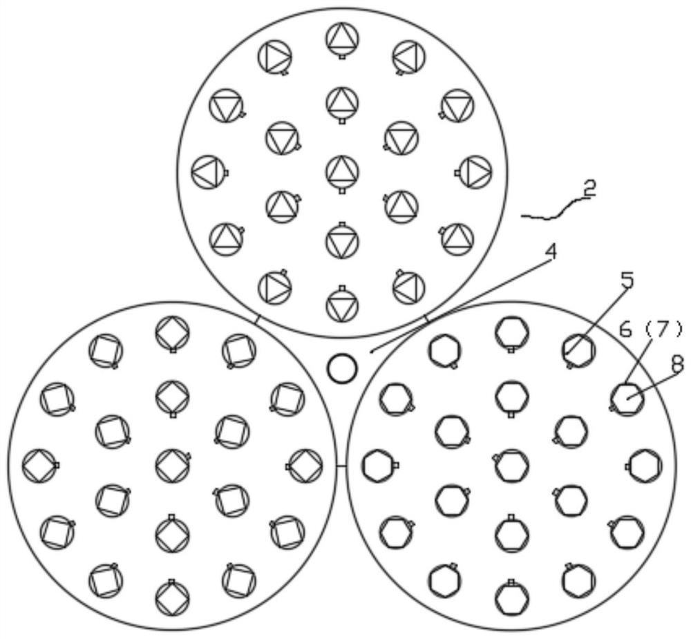
[0030] like figure 1 As shown, the present invention is a texture baffle capable of reducing the residual stress of semiconductor coating, comprising a mounting bracket 1, a texture shape transforming plate 2 and a texture shape shielding plate 3 which are coaxially rotatably arranged on the mounting bracket 1, such as figure 2 As shown, the texture shape changing plate 2 includes a first central connecting plate 4, and three groups of single-textured plates 5 annularly evenly distributed in the circumferential direction of the first central connecting plate 4. 120° evenly distributed. A plurality of first through holes 6 are uniformly arranged on the single-texture board 5 in an array, and a texture module 7 is matched in the first through hole 6. The texture module 7 is provided with a texture through hole 8, and the texture through hole 8 is divided into three shapes. They are triangles, quadrilaterals and hexagons, respectively, and the sandblasting or thermal spraying p...


PUM


Abstract

The invention discloses a texture baffle plate capable of reducing semiconductor coating stress residue, which belongs to the technical field of semiconductor metal vacuum coating and comprises a mounting bracket, a texture shape transformation plate and a texture shape shielding plate, the texture shape transformation plate comprises a first center connecting plate and at least two sets of single texture plates annularly and evenly distributed in the circumferential direction of the first center connecting plate, and a plurality of first through holes are evenly formed in each single texture plate in an array mode. The texture-shaped shielding plate comprises a second center connecting plate and at least two sets of single shielding plates annularly and evenly distributed in the circumferential direction of the second center connecting plate, and a plurality of second through holes are evenly formed in the single shielding plates. The device provided by the invention can provide various texture shapes for a product, so that the regular texture shape and density which are most fit with a processed material can be tested, and guiding significance is made for subsequent stress residue research.

Description

technical field [0001] The invention belongs to the technical field of semiconductor metal vacuum coating, and in particular relates to a texture baffle capable of reducing the residual stress of semiconductor coating. Background technique [0002] Alumina is the most widely used material in advanced ceramics. Because of its high hardness, high temperature resistance, high wear resistance and low density, it is widely used in semiconductor processing equipment, especially in physical thin film deposition technology. In the early days, the film deposition was performed on the initial roughness of the machined ceramic surface, but due to the limited surface roughness of conventional ceramic parts, resulting in residual stress after surface coating, the coating adhesion, uniformity and thickness. restricted. With the continuous development and advancement of the semiconductor process, the control of thin films has become more stringent and the production efficiency has improve...

Claims


Application Information

Patent Timeline
IPC IPC(8): C23C14/02
CPCC23C14/028
Inventor 陈立航屈麟峰廖光洪郑宣杨佐东
Owner 重庆臻宝实业有限公司
Why Eureka
Try Eureka