Insulation protection flip LED chip structure and manufacturing method thereof
A LED chip and insulation protection technology, applied in electrical components, circuits, semiconductor devices, etc., can solve problems such as poor light extraction efficiency, poor safety and energy saving, and achieve the effects of reducing leakage rate, improving performance, and inhibiting water vapor erosion
- Summary
- Abstract
- Description
- Claims
- Application Information
AI Technical Summary
Problems solved by technology
Method used
Image

Examples
Embodiment 1
[0027] The manufacturing method of the insulated and protected flip-chip LED chip structure of the present invention at least includes the following steps:
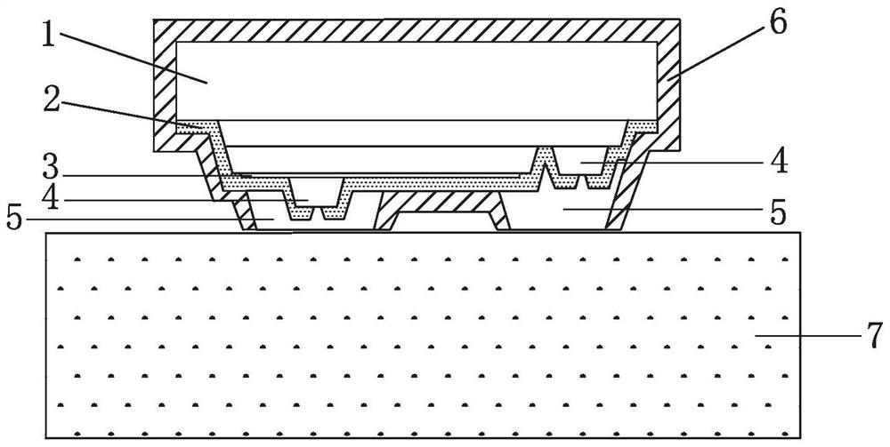
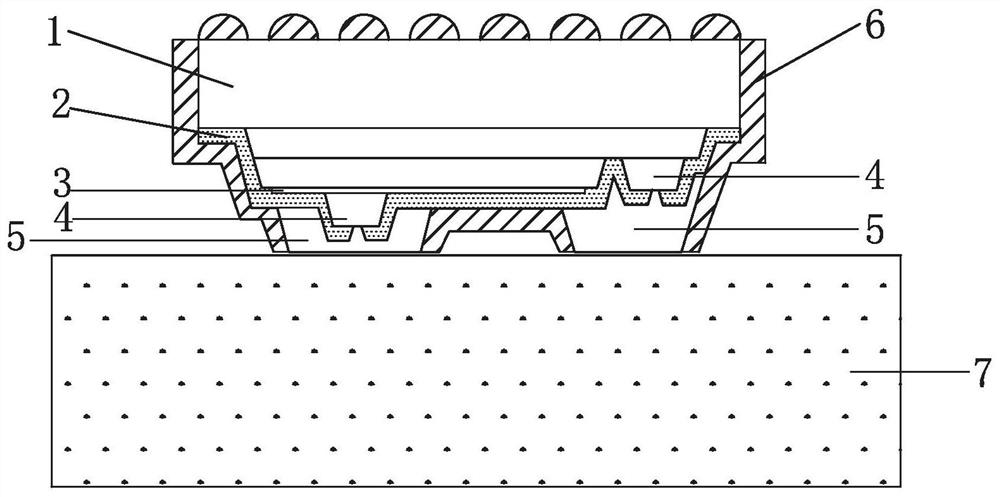
[0028] Step S1 : growing an LED chip epitaxial structure on the chip substrate 1 , and fabricating a chip current layered structure and N, P metal conductive layers 4 . Chip substrate 1 includes but not limited to sapphire, silicon wafer, silicon carbide wafer or metal. For example, the LED chip epitaxial structure is grown on the chip substrate 1 by using MOCVD equipment (MOCVD, metal organic compound chemical vapor deposition). U-GaN layer, N-GaN layer, multi-quantum well layer and P-GaN layer, or N-GaN layer, multi-quantum well layer and P-GaN layer grown in sequence, the LED chip epitaxial structure covers the chip The entire surface of the substrate 1. MOCVD is a new type of vapor phase epitaxy growth technology developed on the basis of vapor phase epitaxy (VPE). The current layered structure includes at least a ...
Embodiment 2
[0033] The manufacturing method of the insulation-protected flip-chip LED chip structure of the present invention at least includes the following steps:
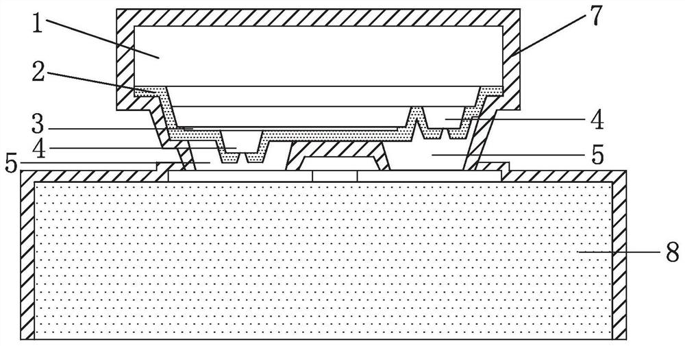
[0034] Step S1 : growing an LED chip epitaxial structure on the chip substrate 1 , and fabricating a chip current layered structure and N, P metal conductive layers 4 . Chip substrate 1 includes but not limited to sapphire, silicon wafer, silicon carbide wafer or metal. For example, the LED chip epitaxial structure is grown on the chip substrate 1 by using MOCVD equipment (MOCVD, metal organic compound chemical vapor deposition). U-GaN layer, N-GaN layer, multi-quantum well layer and P-GaN layer, or N-GaN layer, multi-quantum well layer and P-GaN layer grown in sequence, the LED chip epitaxial structure covers the chip The entire surface of the substrate 1. MOCVD is a new type of vapor phase epitaxy growth technology developed on the basis of vapor phase epitaxy (VPE).
[0035] Use ALD or PECVD coating technology to depos...
PUM
 Abstract
Description
Claims
Application Information
 - R&D
- Intellectual Property
- Life Sciences
- Materials
- Tech Scout
- Unparalleled Data Quality
- Higher Quality Content
- 60% Fewer Hallucinations
Browse by: Latest US Patents, China's latest patents, Technical Efficacy Thesaurus, Application Domain, Technology Topic, Popular Technical Reports.
© 2025 PatSnap. All rights reserved.Legal|Privacy policy|Modern Slavery Act Transparency Statement|Sitemap|About US| Contact US: help@patsnap.com