High-sensitivity light detection device
A light detection device and sensitive technology, applied in the field of light detection, can solve problems such as narrow detection wavelength range, and achieve the effect of wide detection wavelength range and good application prospect.
- Summary
- Abstract
- Description
- Claims
- Application Information
AI Technical Summary
Problems solved by technology
Method used
Image


Examples
Embodiment 1
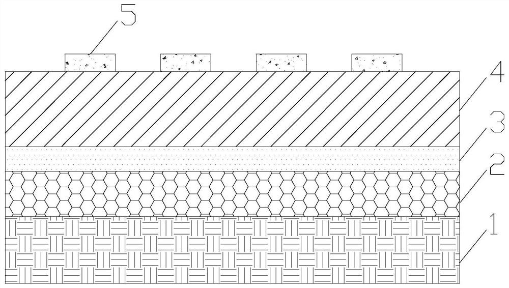
[0024] The invention provides a highly sensitive light detection device. Such as figure 1 As shown, the highly sensitive photodetection device includes an antiferromagnetic layer 1 , a pinning layer 2 , a barrier layer 3 , a free layer 4 , and a noble metal micro-nano structure 5 . The material of the antiferromagnetic layer 1 is a hard magnetic antiferromagnetic material, specifically, the material of the antiferromagnetic layer 1 is IrMn, PtMn, FeMn. The pinning layer 2 is placed on the antiferromagnetic layer 1 . The material of the pinning layer 2 is a metal or semi-metal with high spin polarizability, specifically, the material of the pinning layer 2 is Co, Fe, CoFe, CoFeB, CoFeAl alloy. The barrier layer 3 is placed on the pinning layer 2 . The free layer 4 is placed on the barrier layer 3 . The material of the free layer 4 is soft magnetic material with weak magnetic anisotropy, specifically, the material of the free layer 4 is NiFe alloy, CoFe alloy, CoFeB alloy. ...
Embodiment 2
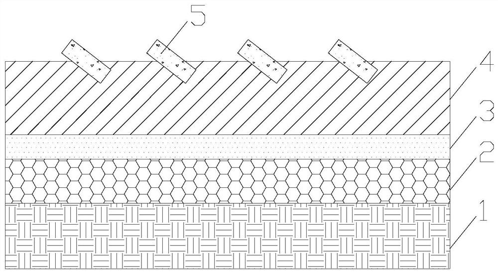
[0028] On the basis of Example 1, such as figure 2 As shown, the noble metal micro-nanostructure 5 is inclined relative to the surface of the free layer 4 , and the noble metal micro-nanostructure 5 is partially placed in the free layer 4 . In this way, on the one hand, the action distance between the noble metal micro-nanostructure 5 and the light to be measured is increased, thereby generating stronger localized surface plasmon resonance on the noble metal micro-nanostructure 5, and thus the noble metal micro-nanostructure 5 On the other hand, since the noble metal micro-nanostructure 5 is partly placed in the free layer 4, the heat transfer between the noble metal micro-nanostructure 5 and the free layer 4 is strengthened, so that the temperature of the free layer 4 Change more. The effects of these two aspects make the spin state of the free layer 4 change more, thereby changing the magnetoresistance of the magnetic tunnel junction more, so as to realize light detection ...
Embodiment 3
[0030] On the basis of Example 1, such as image 3 As shown, a second noble metal micro-nano structure 6 is also included, the second noble metal micro-nano structure 6 is placed in the free layer 4 , and the second noble metal micro-nano structure 6 is connected to the noble metal micro-nano structure 5 . The material of the second noble metal micro-nanostructure 6 is the same as that of the noble metal micro-nanostructure 5 . In this way, localized surface plasmon resonance is formed in the composite structure composed of the noble metal micro-nanostructure 5 and the second noble metal micro-nanostructure 6, and at the junction of the noble metal micro-nanostructure 5 and the second noble metal micro-nanostructure 6 , corners generate more heat, thereby changing the temperature of the free layer 4 more; in addition, because the second noble metal micro-nano structure 6 is placed in the free layer 4, it can also ensure that the heat generated by the above-mentioned composite ...
PUM
| Property | Measurement | Unit |
|---|---|---|
| thickness | aaaaa | aaaaa |
Abstract
Description
Claims
Application Information
 - R&D
- Intellectual Property
- Life Sciences
- Materials
- Tech Scout
- Unparalleled Data Quality
- Higher Quality Content
- 60% Fewer Hallucinations
Browse by: Latest US Patents, China's latest patents, Technical Efficacy Thesaurus, Application Domain, Technology Topic, Popular Technical Reports.
© 2025 PatSnap. All rights reserved.Legal|Privacy policy|Modern Slavery Act Transparency Statement|Sitemap|About US| Contact US: help@patsnap.com