Low dark current pin detector and its processing method

A detector and current technology, applied in sustainable manufacturing/processing, circuits, electrical components, etc., to reduce dark current, weaken diffusion, and improve the effect of use

Inactive Publication Date: 2018-08-31
SUZHOU NORTHEAGLE PHOTONIC SCI TEC
View PDF5 Cites 0 Cited by
  • Summary
  • Abstract
  • Description
  • Claims
  • Application Information

AI Technical Summary

Problems solved by technology

And because the junction depth of the PIN detector is deep, the traditional ion implantation process is difficult to directly apply to the production and processing of the PIN detector.

Method used


Image

  • Low dark current pin detector and its processing method
  • Low dark current pin detector and its processing method
  • Low dark current pin detector and its processing method

Examples


Embodiment Construction

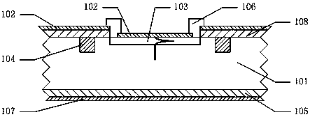
[0038] The invention discloses a low dark current PIN detector.

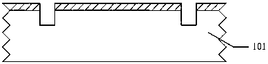
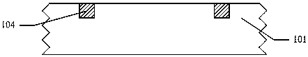
[0039] As shown in the figure, a low dark current PIN detector, which can be used for light detection in the infrared, visible light, ultraviolet or terahertz range, includes a substrate 101, and a P-type ohmic contact layer is grown on the upper surface of the substrate 101 103, the P-type ohmic contact layer 103 is covered with an anti-reflection film 102, and the anti-reflection film 102 is provided with at least one P-type ohmic contact electrode 106 in contact with the P-type ohmic contact layer 103, the The upper end surface of the substrate 101 is provided with a circle of isolation trenches 104 for blocking the internal electric field of the device and the edge of the device. The isolation trenches 104 are located on the outer peripheral side of the P-type ohmic contact layer 103. The isolation trenches 104 is filled with a barrier material, and the upper end surface of the substrate 101 is covered with ...


PUM


Abstract

The invention discloses a low-dark-current PIN detector comprising a substrate. A P-type ohmic contact layer is grown on the upper end surface of the substrate. At least one P-type ohmic contact electrode contacted with the P-type ohmic contact layer is arranged on the P-type ohmic contact layer. An antireflection film of the specific thickness for different wavelength is grown on the upper end surface of the substrate. The upper end surface of the substrate is provided with two isolation grooves which are used for realizing blocking of the internal electric field of a device and the edge of the device. The isolation grooves are arranged at the two sides of the P-type ohmic contact layer. Isolation material is filled in the isolation grooves. A blocking layer covers the area apart from the grooves of the upper end surface of the substrate. An N-type ohmic contact layer and N-type ohmic contact electrodes are grown on the lower end surface of the substrate from the top to the bottom in turn in a covering way. Dark current in the device can be effectively reduced and the use effect is excellent so that the low-dark-current PIN detector has extremely high use and popularization value.

Description

technical field [0001] The invention relates to a photoelectric detector, in particular to a low dark current PIN detector, which belongs to the field of semiconductor photoelectric devices. Background technique [0002] As an important "carrier" to realize optical signal detection, PIN detector has the advantages of simple process, high detection efficiency and stable performance. It plays an important supporting role and is the commanding height for various countries to seize. For example, in high-energy radiography such as security inspection and medical treatment, PIN photodetectors cooperate with scintillators to realize the process of converting weak light signals into electrical signals and outputting imaging. [0003] The dark current of PIN detectors can be divided according to the relationship with the device size: the line dark current related to the circumference, the surface dark current related to the area, and the dark current compensation not related to the ...

Claims


Application Information

Patent Timeline
Patent Type & Authority Patents(China)
IPC IPC(8): H01L31/105H01L31/18
CPCH01L31/105H01L31/18Y02P70/50
Inventor 李冲丰亚洁刘巧莉吕本顺郭霞王华强黎奔
Owner SUZHOU NORTHEAGLE PHOTONIC SCI TEC
Why Eureka
Try Eureka