Ultrafast micro-LED of MIS structure based on local surface plasmon coupling enhancement and production method of ultrafast micro-LED

A technology of localized surface plasmon and MIS structure, applied in electrical components, circuits, semiconductor devices, etc., can solve the problem of low modulation bandwidth, and achieve the effects of increasing modulation bandwidth, simple preparation process, and improving recombination rate and recombination efficiency.

Pending Publication Date: 2021-10-01
XIAMEN UNIV
View PDF5 Cites 1 Cited by
  • Summary
  • Abstract
  • Description
  • Claims
  • Application Information

AI Technical Summary

Problems solved by technology

[0007] In order to solve the problem of low modulation bandwidth of micro-LEDs with MIS structure, the present invention provides an ultrafast micro-LED with MIS structure based on localized surface plasmon coupling enhancement, which utilizes localized surface plasmons The near-field coupling enhancement effect can effectively improve the carrier recombination rate and recombination efficiency of the device and improve the luminous efficiency at the same time, forming an efficient and fast micro-LED, and the effective carrier recombination time is significantly reduced, which greatly improves the modulation bandwidth and can expand Application of micro-LED in visible light communication

Method used


Image

  • Ultrafast micro-LED of MIS structure based on local surface plasmon coupling enhancement and production method of ultrafast micro-LED
  • Ultrafast micro-LED of MIS structure based on local surface plasmon coupling enhancement and production method of ultrafast micro-LED

Examples


preparation example Construction

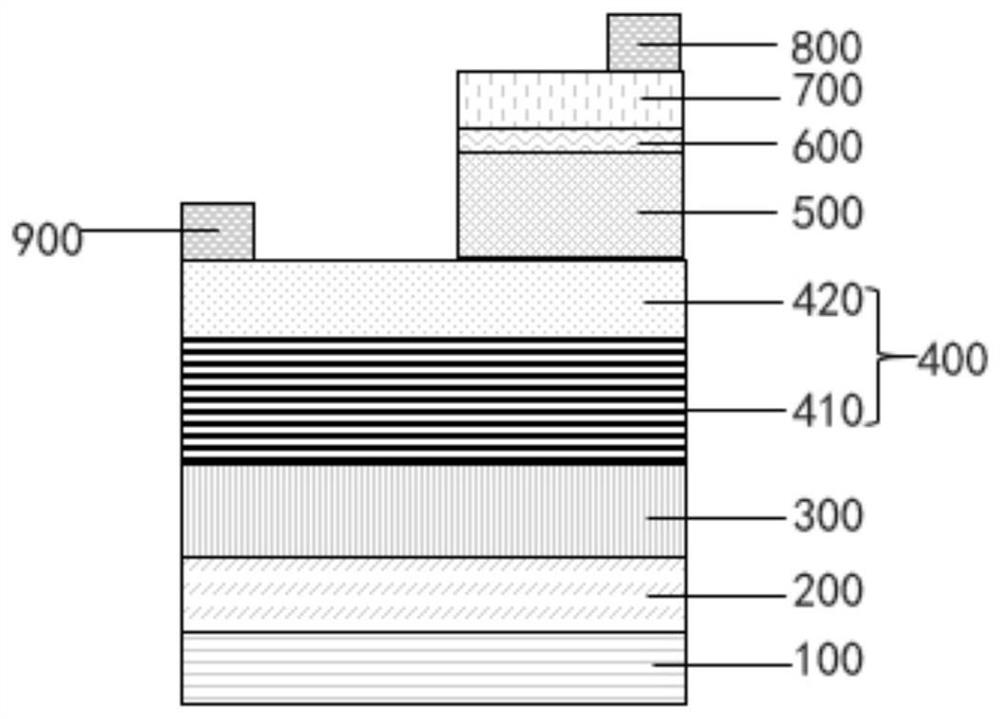
[0053] The present invention also provides a method for preparing an ultrafast micro-LED based on a localized surface plasmon coupling enhanced MIS structure as described above, which includes the following steps:

[0054] S100. Using metal-organic vapor phase epitaxy technology to grow a low-temperature buffer layer on the substrate, and then raise the temperature to grow a high-temperature gallium nitride layer on the buffer layer;

[0055] S200, continue to use metal-organic vapor phase epitaxy technology to grow a p-type active layer on the gallium nitride layer;

[0056] S300. Depositing an insulating layer on the p-type active layer by using plasma-enhanced chemical vapor deposition technology;

[0057] S400, using a chemical wet etching process to transfer the current spreading layer, and growing the current spreading layer on the surface of the insulating layer;

[0058] S500. Evaporating a metal thin film layer on the surface of the current spreading layer by using t...

Embodiment 1

[0065] The present invention provides as Figure 1-2 The specific structure of the ultrafast micro-LED based on the localized surface plasmon coupling enhanced MIS structure shown in Example 1, and its preparation method is as follows:

[0066] Among them, in the preparation process, trimethylaluminum (TMAl) and trimethylgallium (TMGa) were used as group III sources, ammonia (NH3) was used as group V sources, and dipentyl magnesium (Cp2Mg) was used as p-type active layer doping agent, high-purity hydrogen as the carrier gas.

[0067] 1) growing the buffer layer 200 and the gallium nitride layer 300, specifically:

[0068] 1.1) Using metal organic vapor phase epitaxy technology, before growing epitaxy, place sapphire substrate 100 in H 2 In the atmosphere, remove the contamination on the surface at a high temperature of 1100°C and a reaction chamber pressure of 100Torr; after lowering the temperature to 800°C, feed TMGa and NH under a reaction chamber pressure of 500Torr 3 ,...


PUM

PropertyMeasurementUnit
diameteraaaaaaaaaa
thicknessaaaaaaaaaa
thicknessaaaaaaaaaa

Abstract

The invention relates to the field of photoelectric semiconductors, and particularly relates to an ultrafast micro-LED of an MIS structure based on local surface plasmon coupling enhancement and a production method of the ultrafast micro-LED. The micro-LED sequentially comprises a substrate, a buffer layer, a gallium nitride layer, a p-type active layer, an insulating layer, a current expansion layer and a metal nanoparticle structure from bottom to top, an opening extending to the surface of the p-type active layer is formed in the surface of the metal nanoparticle structure so that an exposed area is formed on the surface of the p-type active layer, a p-type ohmic contact electrode is arranged on the surface of the exposed area, and an n-type ohmic contact electrode is arranged on the surface of the metal nanoparticle structure. According to the micro-LED provided by the invention, the carrier recombination rate and recombination efficiency of the device can be effectively improved, and the service life of effective carriers is shortened so that the modulation bandwidth of the device is greatly increased, and the application of the micro-LED in optical communication is expanded.

Description

technical field [0001] The invention relates to the field of optoelectronic semiconductors, in particular to an ultrafast micro-LED based on a localized surface plasmon coupling enhanced MIS structure and a preparation method thereof. Background technique [0002] At present, wide bandgap semiconductor light sources have been widely used and concerned in the fields of lighting, sterilization, medical treatment, biochemical detection, and secure communication. Micro-LED has a series of advantages such as high resolution, high resolution, high image quality, low energy consumption, high brightness, fast response, long working life, stability and reliability, and high efficiency, making it widely used in the field of display technology, optical communication, etc. Many application fields such as optogenetics and optogenetics have shown good application prospects, and are widely considered to be the next major trend in the field of display technology. [0003] The structure of ...

Claims


Application Information

Patent Timeline
Patent Type & Authority Applications(China)
IPC IPC(8): H01L33/06H01L33/04H01L33/14H01L33/00
CPCH01L33/06H01L33/04H01L33/14H01L33/0037
Inventor 黄凯王丽兰李金钗高娜江莹康俊勇张荣
Owner XIAMEN UNIV
Why Eureka
Try Eureka