Additive for copper catalytic etching silicon wafer etching liquid, etching system and etching method
An additive and copper-catalyzed technology, applied in the field of solar photovoltaics, can solve the problems of fast reaction rate, uneven etching rate, and high loss of silicon materials, and achieve uniform and smooth structure, appropriate etching reaction rate, and weight reduction rate. The effect of low reflectivity
- Summary
- Abstract
- Description
- Claims
- Application Information
AI Technical Summary
Problems solved by technology
Method used
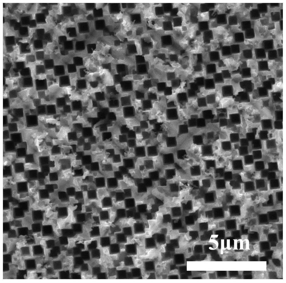
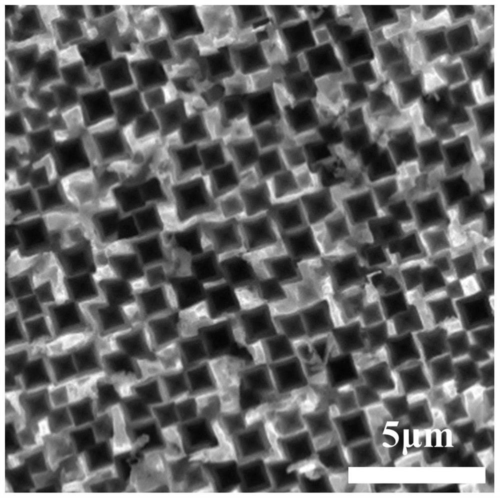
Image

Examples
Embodiment 1
[0029] An additive for copper catalyzed etching silicon chip etching solution, which is a solution including a metal complexing agent and an acidity regulator. Among them, the metal complexing agent (also known as metal chelating agent, metal chelating agent) can clathrate the metal ion into the complexing agent through the strong combination between the complexing agent molecule and the metal ion, and become stable and have a larger molecular weight. Compounds, thus preventing metal ions from acting, are commonly used in printing and dyeing, scale inhibition and other fields in industry. Based on the characteristic of the metal complexing agent, the present invention introduces it as an additive into the copper-catalyzed etching silicon wafer etching solution, and is used to control and slow down the etching reaction rate, so as to solve the problem that the reaction rate of the copper-catalyzed chemical etching method is too fast, making the silicon material The technical pr...
Embodiment 2
[0034] The etching system for copper-catalyzed etching of silicon wafers is obtained by mixing the additives in Example 1 with a copper-catalyzed etching solution, wherein the etching solution includes: metal copper salt, oxidizing agent, etchant and water.
[0035] In a preferred embodiment, the metal copper salt includes: one of copper nitrate, copper chloride or copper sulfate; the oxidizing agent includes: hydrogen peroxide or nitric acid; the etchant is hydrofluoric acid; preferably, the concentration of the metal copper salt The concentration of the etchant is between 0.01mol / L and 0.5mol / L, the concentration of the etchant is between 0.01mol / L and 0.5mol / L, and the concentration of the oxidizing agent is between 0.1mol / L and 3mol / L.
[0036] In a preferred embodiment, the mass ratio of the additive to the etching solution is 0.1-6:100, preferably 0.1-3.0:100. By adding a small amount of the additive of the present invention to the etching solution in the prior art, the ...
Embodiment 3
[0038] The etching method for silicon wafer texturing adopts the copper-catalyzed etching silicon wafer etching system obtained in Example 2, including: an etching step, immersing the silicon wafer in the etching system for etching.
[0039]In a preferred embodiment, the etching temperature is between 20°C to 70°C, preferably 30°C to 50°C, more preferably 40°C; the etching time is between 1min to 30min, preferably 3min to 15min, More preferably, it is 12 minutes. It can be seen that the formula provided in the preferred embodiment of the present invention can carry out the etching reaction at a temperature that is more gentle and easy to control, and the etching time is within half an hour, and the etching reaction rate is appropriate, which avoids etching If the etching reaction rate is too fast, the etching process is difficult to control, and the etching reaction rate is not too slow, so that the etching time is too long, resulting in an increase in the cost caused by low e...
PUM
| Property | Measurement | Unit |
|---|---|---|
| thickness | aaaaa | aaaaa |
| quality score | aaaaa | aaaaa |
Abstract
Description
Claims
Application Information
 - Generate Ideas
- Intellectual Property
- Life Sciences
- Materials
- Tech Scout
- Unparalleled Data Quality
- Higher Quality Content
- 60% Fewer Hallucinations
Browse by: Latest US Patents, China's latest patents, Technical Efficacy Thesaurus, Application Domain, Technology Topic, Popular Technical Reports.
© 2025 PatSnap. All rights reserved.Legal|Privacy policy|Modern Slavery Act Transparency Statement|Sitemap|About US| Contact US: help@patsnap.com