Single-photon detector and preparation method
A single-photon detector, superconducting wire technology, applied in the field of light detection, can solve problems affecting device performance, current crowding effect, etc.
- Summary
- Abstract
- Description
- Claims
- Application Information
AI Technical Summary
Problems solved by technology
Method used
Image
Examples
Embodiment 1
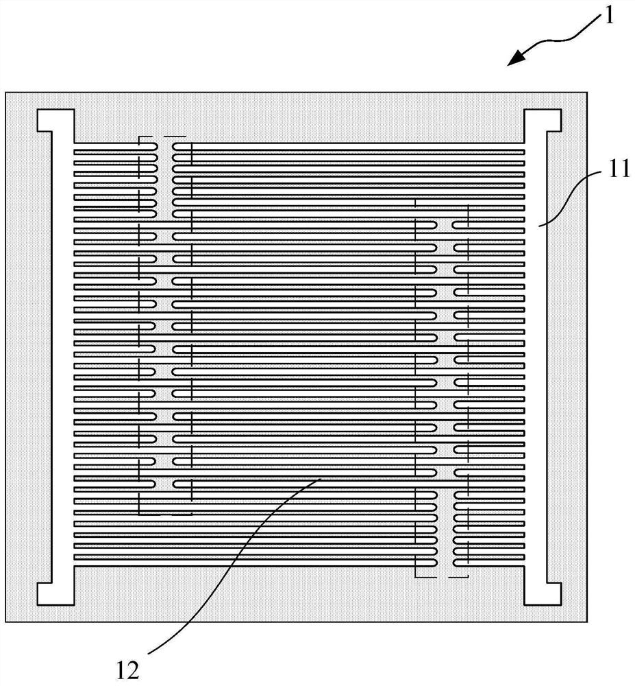
[0050] Such as Figure 1 ~ Figure 3 As shown, the present embodiment provides a single photon detector 1, and the single photon detector includes:
[0051] Substrate 11 and superconducting wire 12.
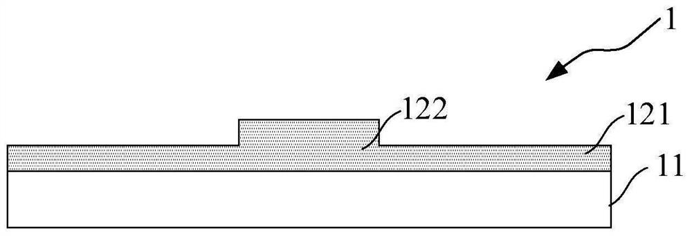
[0052] Such as image 3 As shown, the substrate 11 is located at the bottom of the single photon detector 1 .
[0053] Specifically, the substrate 11 includes but is not limited to a silicon substrate, a MgO substrate or a sapphire substrate. As an example, the substrate 11 is a silicon substrate.
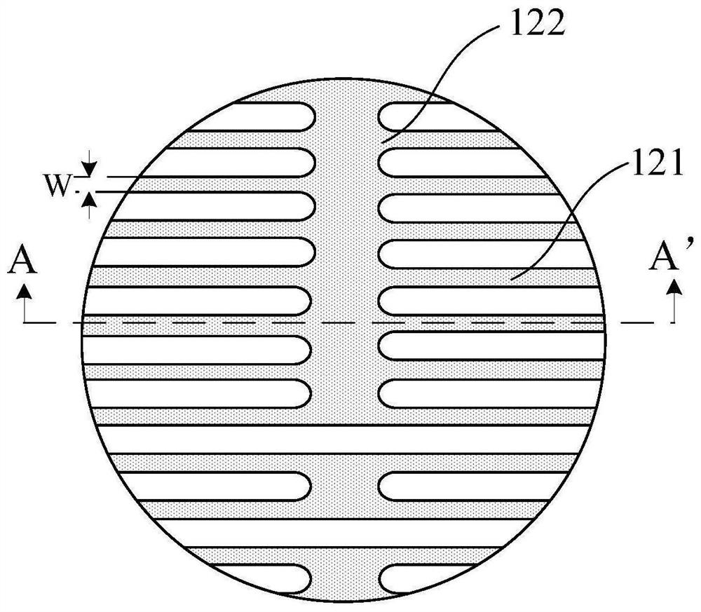
[0054] Such as Figure 1 ~ Figure 3 As shown, the superconducting wire 12 is formed on the substrate 11 , and the superconducting wire 12 includes a plurality of straight portions 121 and corner portions 122 connecting the straight portions 121 .
[0055] Specifically, the material of the superconducting wire includes but is not limited to NbN, Nb, NbSi, WSi, TaN, MoSi or NbTiN. As an example, the superconducting wire is made of NbN. The superconducting wire 12 is a superconductin...
Embodiment 2
[0064] Such as Figure 10 As shown, this embodiment provides a preparation method of the single photon detector of the first embodiment, the preparation method of the single photon detector includes:
[0065] 1) A substrate 11 is provided, and a first superconducting thin film is grown on the surface of the substrate 11 .
[0066] Specifically, a substrate 11 is firstly provided, and a first superconducting thin film (NbN material is selected in this embodiment) for preparing SNSPD is grown on the front surface of the substrate 11 by using a high vacuum magnetron sputtering device.
[0067] 2) Spin-coat photoresist on the first superconducting thin film, expose the corner area of the superconducting wire through exposure and development, and remove the oxide layer on the surface of the corner area.
[0068] Specifically, in this embodiment, it also includes spin-coating electron beam exposure glue PMMA (that is, photoresist) on the surface of the first superconducting thin ...
PUM
| Property | Measurement | Unit |
|---|---|---|
| current density | aaaaa | aaaaa |
| current density | aaaaa | aaaaa |
Abstract
Description
Claims
Application Information
 - R&D Engineer
- R&D Manager
- IP Professional
- Industry Leading Data Capabilities
- Powerful AI technology
- Patent DNA Extraction
Browse by: Latest US Patents, China's latest patents, Technical Efficacy Thesaurus, Application Domain, Technology Topic, Popular Technical Reports.
© 2024 PatSnap. All rights reserved.Legal|Privacy policy|Modern Slavery Act Transparency Statement|Sitemap|About US| Contact US: help@patsnap.com


