Method and device for preparing passivation contact solar cell by plate-type equipment
A solar cell and panel technology, applied in circuits, photovoltaic power generation, electrical components, etc., can solve problems such as expensive machines, inconsistent process temperatures, and complicated processes, and achieve reduced phosphorus doping processes, reduced cleaning steps, and low process temperatures Effect
- Summary
- Abstract
- Description
- Claims
- Application Information
AI Technical Summary
Problems solved by technology
Method used
Image
Examples
Embodiment 1
[0064] This embodiment 1 takes the preparation of an N-type passivated contact structure battery as an example, which includes the following steps:
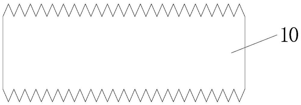
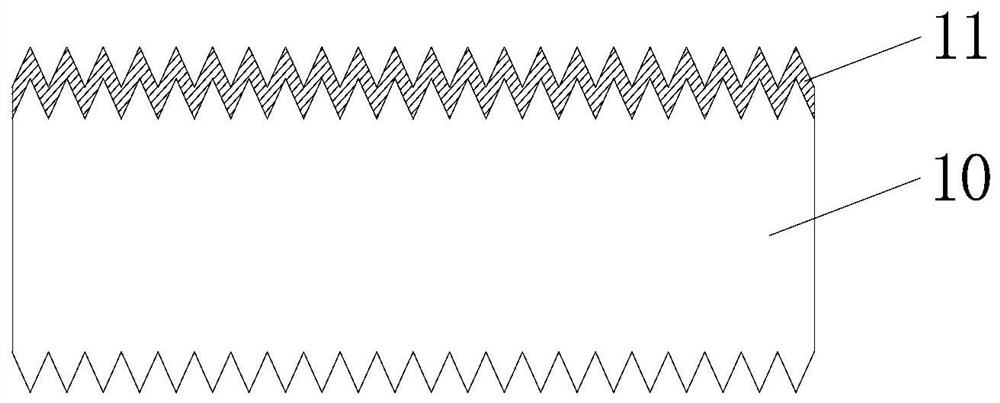
[0065] S1. Select Picture 1-1 The shown N-type crystalline silicon substrate 10 has a resistivity of 0.3-5 Ω cm and a thickness of 80-200 μm, and then alkali texturing is performed on the surface of the N-type crystalline silicon substrate 10 to obtain Figure 1-2 The double-sided textured structure shown, and the front textured surface of the N-type crystalline silicon substrate 10 adopts BBr 3 Gaseous Source Diffusion Formation Figure 1-3 The shown N-type crystalline silicon substrate 10 with a boron diffusion layer 11 forms a PN junction with a square resistance of 80~200Ω / □, and then removes borosilicate glass (BSG) impurities on the surface by cleaning;
[0066] S2. After the N-type crystalline silicon substrate 10 pretreated in step S1 is tiled on image 3 The shown 4×4 specification carrier plate 30 is transported to a...
Embodiment 2
[0073] In Example 2, the preparation of a PERC battery with a P-type passivation contact structure is taken as an example, which includes the following steps:
[0074] S1. Select diagram 2-1 The P-type crystalline silicon substrate 20 shown has a resistivity of 0.1-5 Ω cm and a thickness of 80-200 μm, and then alkali texturing is performed on the surface of the P-type crystalline silicon substrate 20 to obtain Figure 2-2 Double sided textured construction shown with POCl on one sided textured surface 3 Gaseous Source Diffusion Formation Figure 2-3 The shown P-type crystalline silicon substrate 20 with phosphorus diffusion layer 21 forms a PN junction with a square resistance of 40-200Ω / □, and then removes phosphosilicate glass (PSG) impurities on the surface by cleaning;
[0075] S2. After the P-type crystalline silicon substrate 20 pretreated in step S1 is tiled on image 3 The shown 4×4 specification carrier plate 30 is transported to a plate-type integrated continuous...
PUM
| Property | Measurement | Unit |
|---|---|---|
| thickness | aaaaa | aaaaa |
| electrical resistivity | aaaaa | aaaaa |
| thickness | aaaaa | aaaaa |
Abstract
Description
Claims
Application Information
 - R&D
- Intellectual Property
- Life Sciences
- Materials
- Tech Scout
- Unparalleled Data Quality
- Higher Quality Content
- 60% Fewer Hallucinations
Browse by: Latest US Patents, China's latest patents, Technical Efficacy Thesaurus, Application Domain, Technology Topic, Popular Technical Reports.
© 2025 PatSnap. All rights reserved.Legal|Privacy policy|Modern Slavery Act Transparency Statement|Sitemap|About US| Contact US: help@patsnap.com


