Anti-ferroelectric ceramic material and low-temperature sintering method thereof
A ceramic material, low temperature sintering technology, applied in the field of functional ceramics, can solve problems such as increasing the manufacturing cost of multilayer capacitors, and achieve the effect of simple, economical and practical preparation method
- Summary
- Abstract
- Description
- Claims
- Application Information
AI Technical Summary
Problems solved by technology
Method used
Image

Examples
Embodiment 1
[0036] In this embodiment, the general chemical formula is PbZrO 3 The antiferroelectric ceramic material, the sintering aid is Ag 2 O powder, its preparation method comprises the following steps:
[0037] 1) Select Pb with a purity greater than 99% 3 o 4 , ZrO 2 As the raw material of the antiferroelectric ceramic material, it is weighed and mixed according to the chemical composition to obtain the mixture;
[0038] 2) After the mixture is ball milled for 15 hours, discharged, dried, and calcined at 900°C for 3 hours, calcined powder is obtained;
[0039] 3) The calcined powder and 0.5wt.% Ag 2 After O mixing, after secondary ball milling, discharging and drying, dry powder is obtained;
[0040] 4) Mix the dry powder with 8wt% polyvinyl alcohol solution (the mass-to-volume ratio of the mixing process is 0.3mL polyvinyl alcohol solution / g dry powder), and then successively undergo granulation and compression molding at 6MPa to obtain a ceramic embryo body;
[0041] 5) Pl...
Embodiment 2
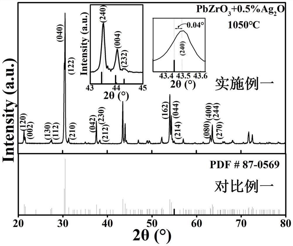
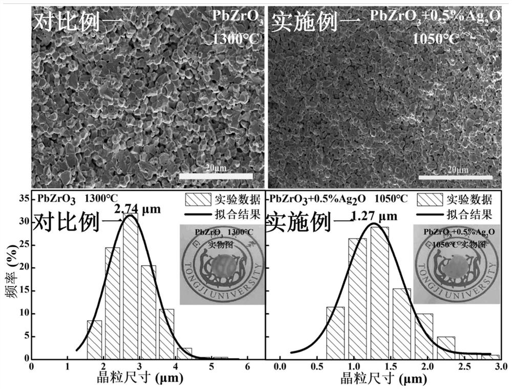
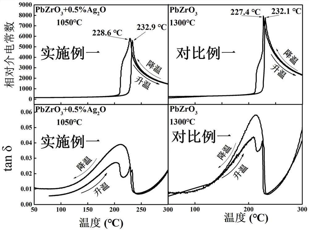
[0043] In this example, the antiferroelectric ceramic materials prepared in Example 1 and Comparative Example 1 were characterized by XRD, SEM, and dielectric spectrum, and the characterization results were as follows: Figure 1 to Figure 3 shown.
[0044] From figure 1 It can be seen that the antiferroelectric ceramic materials prepared in Example 1 all have a single perovskite structure. Moreover, the splitting of the peak near 38° and the splitting of the peak near 44° (three splitting peaks) indicate that the antiferroelectric ceramic prepared in Example 1 has an orthorhombic phase structure. In addition, comparative example 1 is pure PbZrO 3 For ceramics, its XRD pattern is given in a standard PDF card (PDF#87-0569). figure 1 It can be seen from the figure that the position of each diffraction peak in Example 1 is basically consistent with that of Comparative Example 1 (in fact, it only shifts to the high angle by about 0.04°), indicating that the externally doped Ag ...
Embodiment 3
[0048] In this example, the antiferroelectric ceramic materials prepared in Example 1 and Comparative Example 1 were respectively polished with sandpaper of different sizes to obtain a thin ceramic sheet with a smooth surface and a thickness of 0.1mm, and then sprayed the thin ceramic sheet Gold, to obtain a gold electrode with a diameter of 2 mm, and then put the gold electrode in a muffle furnace for heat treatment, that is, bake it at 200 ° C for 0.5 h, and obtain the corresponding samples to be tested.
[0049] Characterize the energy storage performance of the two samples to be tested, such as Figure 4 and Figure 6 is the hysteresis loop of the sample to be tested, such as Figure 5 and Figure 7 Shown is a comparison chart of energy storage density and energy storage efficiency calculated based on the hysteresis loop. It can be seen from the figure that the breakdown electric field strength of the sample to be tested in Example 1 is 330kV / cm, and the maximum polariza...
PUM
| Property | Measurement | Unit |
|---|---|---|
| particle size | aaaaa | aaaaa |
| particle size | aaaaa | aaaaa |
| thickness | aaaaa | aaaaa |
Abstract
Description
Claims
Application Information
 - R&D
- Intellectual Property
- Life Sciences
- Materials
- Tech Scout
- Unparalleled Data Quality
- Higher Quality Content
- 60% Fewer Hallucinations
Browse by: Latest US Patents, China's latest patents, Technical Efficacy Thesaurus, Application Domain, Technology Topic, Popular Technical Reports.
© 2025 PatSnap. All rights reserved.Legal|Privacy policy|Modern Slavery Act Transparency Statement|Sitemap|About US| Contact US: help@patsnap.com