
Preparation method of inorganic CsPbxSn<1-x>(BryI<1-y>)3 nanowire and photoelectric detector thereof

A nanowire and inorganic technology, applied in the field of preparation of inorganic CsPbxSn1-x3 nanowires, can solve the problems of poor performance of perovskite photodetectors and insoluble ions, and achieve controllable metal ion content and low operator requirements , Ease of industrial mass production

Inactive Publication Date: 2020-11-17
HUBEI UNIV
View PDF5 Cites 0 Cited by
  • Summary
  • Abstract
  • Description
  • Claims
  • Application Information

AI Technical Summary

Problems solved by technology

[0003] However, the problem we have to face now is that divalent Sn ions are easily oxidized to tetravalent Sn ions in the air, and the Sn-containing 4+ Perovskite photodetectors perform very poorly
But sn 4+ The problem with ionic is still unresolved

Method used

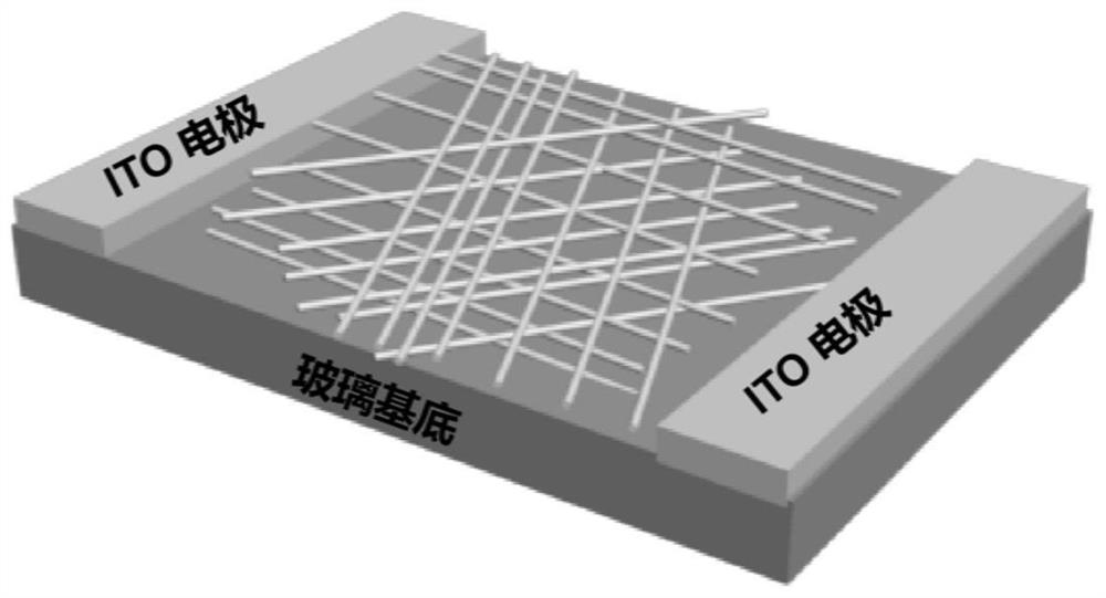
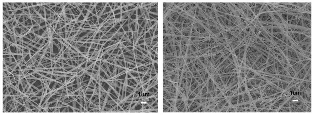
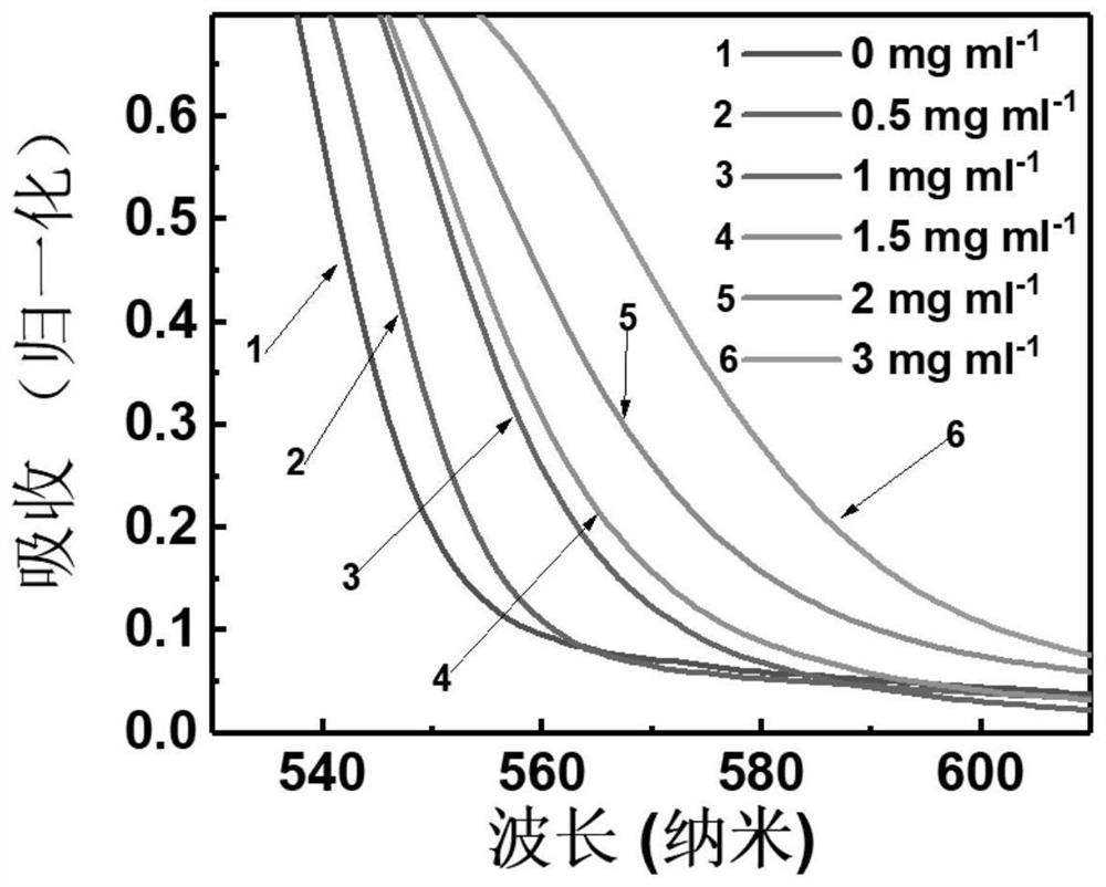

Image

  • Preparation method of inorganic CsPbxSn&lt;1-x&gt;(BryI&lt;1-y&gt;)3 nanowire and photoelectric detector thereof
  • Preparation method of inorganic CsPbxSn&lt;1-x&gt;(BryI&lt;1-y&gt;)3 nanowire and photoelectric detector thereof
  • Preparation method of inorganic CsPbxSn&lt;1-x&gt;(BryI&lt;1-y&gt;)3 nanowire and photoelectric detector thereof

Examples


Embodiment 1

[0030] The present invention will be described in detail below in conjunction with the accompanying drawings and embodiments, and the described embodiments are only some of the embodiments of the present invention, not all of them. Based on the implementation manners in the present invention, all other implementation manners obtained by persons of ordinary skill in the art without creative efforts fall within the protection scope of the present invention. Example 1 This case is to prepare different Sn 2+ Concentration of CsPb x sn 1-x Br 3 Nanowires.

[0031] (1) Clean the substrate

[0032] Select a square glass sheet with a thickness of 1mm, a side length of 2cm, and a channel width of 50um as the substrate (referred to as channel ITO). Use a cotton swab dipped in absolute ethanol to clean the substrate, rinse it with deionized water, and then separate Ultrasonic cleaning with deionized water, acetone and absolute ethanol for 30 minutes each;

[0033] (2) UV ozone trea...

Embodiment 2

[0042] This case is for the preparation of Sn 2+ The concentration is 0.5mg / ml, different Br - Ionic concentration of CsPb x sn 1-x (Br y I 1-y ) 3 Nanowires

[0043] (1) Clean the substrate

[0044] Select a square glass sheet with a thickness of 1mm, a side length of 2cm, and a channel width of 50um as the substrate (referred to as channel ITO). Use a cotton swab dipped in absolute ethanol to clean the substrate, rinse it with deionized water, and then separate Ultrasonic cleaning with deionized water, acetone and absolute ethanol for 30 minutes each;

[0045] (2) UV ozone treatment substrate

[0046] Dry the cleaned substrate with nitrogen, and then put it into a UV ozone cleaning device (PSD-UV4) for 60 minutes of ultraviolet ozone treatment to improve the adhesion of the substrate surface;

[0047] (3) Prepare the solution

[0048] 1 mmol of lead iodide (PbI 2 ) was dissolved in 1ml of N,N-dimethylformamide (DMF), stored in a 70°C oven at a constant temperature...


PUM

PropertyMeasurementUnit
concentrationaaaaaaaaaa

Abstract

The invention discloses a preparation method of an inorganic CsPbxSn<1-x>(BryI<1-y>)3 nanowire and application thereof in a photoelectric detector. The method comprises the following steps: sequentially spin-coating a lead iodide DMF solution on the surface of a conductive glass substrate at room temperature to form a film, and annealing to obtain a PbI2 film; carefully putting the film into a closed culture dish of an absolute methanol solution mixed with cesium iodide and stannous iodide, standing for 3-6 hours, taking out, cleaning with isopropanol, and air-drying; placing place the productin a culture dish containing an absolute methanol solution of cesium bromide for 0-120 minutes, taking out the product, cleaning, air-drying and annealing; and coating a layer of chlorobenzene solution of PMMA on the product in a spinning manner, and annealing to obtain the inorganic CsPbxSn<1-x>(BryI<1-y>)3 nanowire. The preparation method is simple to operate, low in cost and good in stability;performance parameters are similar to those of a full-lead perovskite nanowire photoelectric detector. The Sn element is successfully used for partially replacing the Pb element, the toxicity of perovskite is reduced, and a far-reaching influence is brought to the development of perovskite photoelectric devices.

Description

technical field [0001] The invention belongs to the preparation of perovskite nanostructured inorganic metal halide nanomaterials and its application in optoelectronic devices, in particular to a solution method for preparing inorganic CsPb x Sn 1-x (Br y I 1-y ) 3 Preparation method of nanowire and its application in photodetector. Background technique [0002] In recent years, organic-inorganic hybrid lead halide perovskite materials have become a research hotspot in the field of optoelectronics due to their tunable band gap and simple fabrication. Process and photoelectric conversion efficiency are high. So far, the photoelectric conversion efficiency (PCE) of perovskite solar cells has exceeded 23%. Perovskite-based light-emitting diodes have exceeded 20%. For perovskite-based photodetectors (PDs), the detection rate is as high as 7 × 10 15 Jones. Despite the advancement of technology, the commercialization of perovskite-based devices still faces enormous challe...

Claims


Application Information

Patent Timeline
Patent Type & Authority Applications(China)
IPC IPC(8): C03C17/42C01G21/00H01L31/18H01L31/032
CPCC03C17/42C01G21/006H01L31/18H01L31/032C01P2002/72C01P2004/03C01P2002/84C01P2004/16Y02P70/50
Inventor 周海汤晓明王浩
Owner HUBEI UNIV
Learn More