Production method of two-dimensional crystal forbidden band fluorescence polarization modulation device
A two-dimensional crystal and fluorescence polarization technology, which is applied in the field of nano-optoelectronics, can solve the problems of two-dimensional crystals with small band gap fluorescence polarization modulation and limited by temperature, and achieve the effects of widening the temperature application range, improving device life, and small size
- Summary
- Abstract
- Description
- Claims
- Application Information
AI Technical Summary
Problems solved by technology
Method used
Image
Examples
preparation example Construction
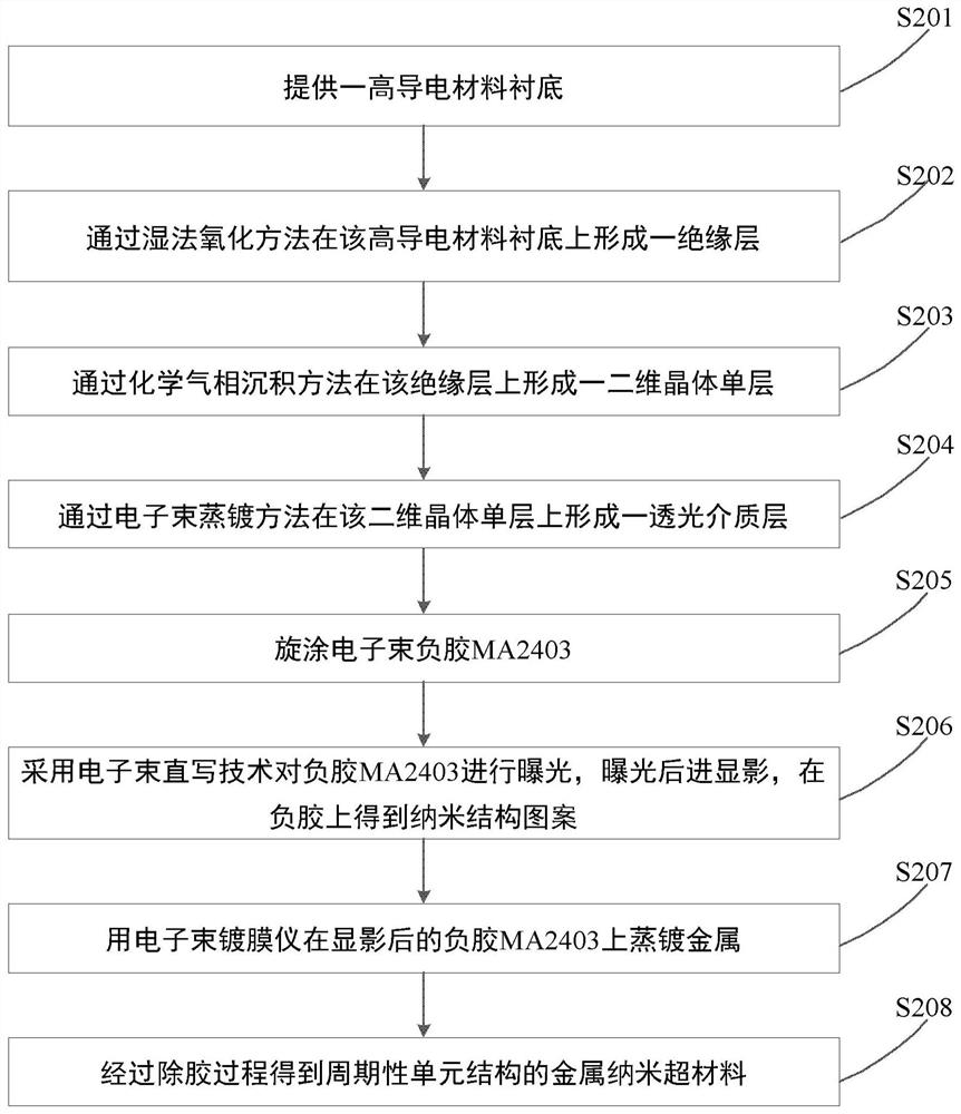
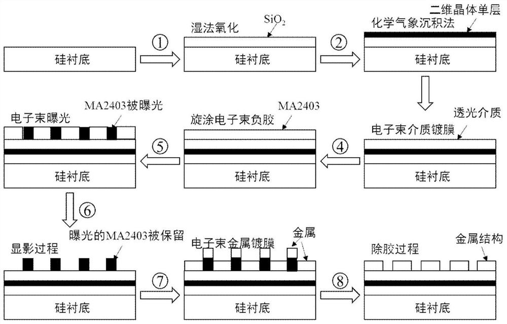
[0070] The invention provides a method for preparing a two-dimensional crystal bandgap fluorescence polarization modulation device. The preparation method is as follows: figure 1 As shown, its preparation process is as follows figure 2 shown, including:
[0071] Step S201: providing a highly conductive material substrate;
[0072] Step S202: Oxidizing an insulating layer on the highly conductive material substrate;
[0073] Step S203: depositing a two-dimensional crystal monolayer on the insulating layer;
[0074] Step S204: Evaporating a light-transmitting medium layer on the two-dimensional crystal monolayer;
[0075] Step S205: spin-coating electron beam negative glue on the light-transmitting medium layer;
[0076] Step S206: exposing the negative film, and developing after exposure;
[0077] Step S207: Evaporating a metal layer on the developed negative film; and
[0078] Step S208 : the metal nano-metamaterial with periodic unit structure on the light-transmitting...
Embodiment 1
[0093] Example 1: WS 2 Monolayer Fluorescence Polarization Test
[0094] First, on SiO 2 / Si substrate, WS was formed by chemical vapor deposition 2 Single layer: heat the powders of sulfur and tungsten to generate steam, and use argon as a carrier gas to bring the steam to a clean substrate for deposition and growth to obtain WS 2 single layer.
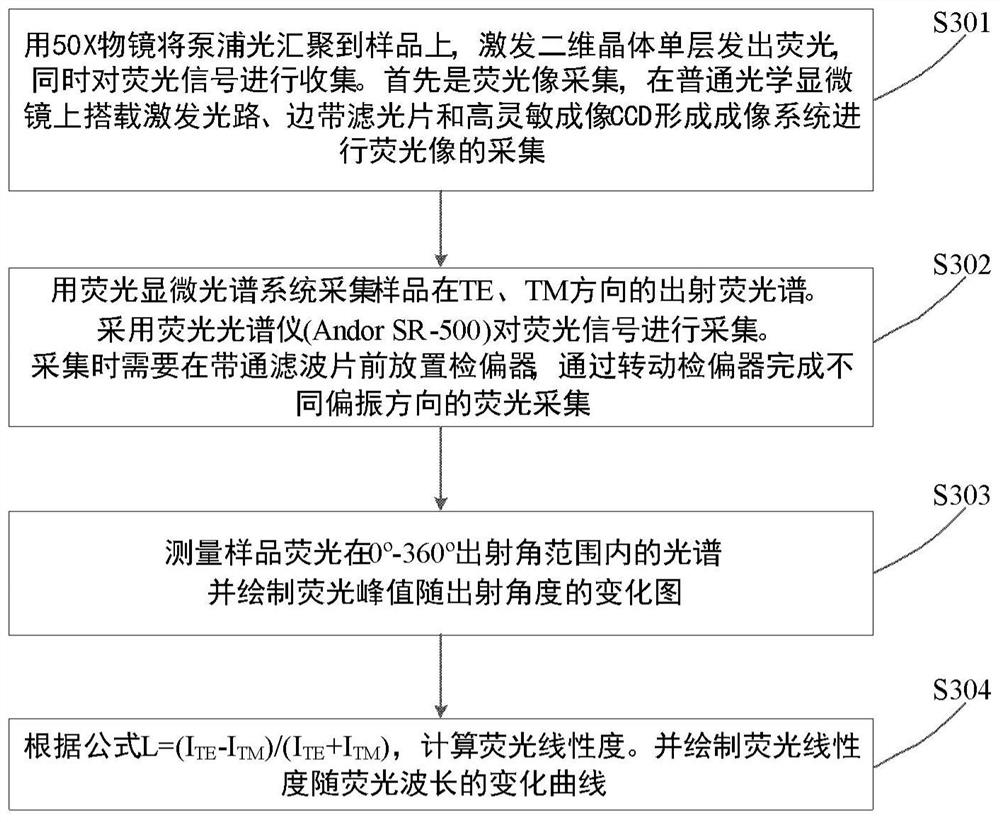
[0095] Figure 4A is the WS 2 Optical microscopy imaging of monolayers. Figure 4B is the emission fluorescence spectrum in the TE and TM directions obtained through the test in step S302. Depend on Figure 4B It can be seen that the fluorescence intensity of the sample is equal in the directions of TE and TM, and WS 2 The fluorescence peak of the monolayer is at ~630nm, the full width at half maximum is ~30nm, and the forbidden band width is 1.9-2.0eV. Figure 4C It is a diagram of the variation of the fluorescence spectrum with the exit angle obtained through the test in step S303. Depend on Figure 4C It can be seen tha...
Embodiment 2
[0096] Example 2: Ag nanowire grid modulation two-dimensional crystal WS 2 bandgap fluorescence polarization
[0097] Since the modulation method proposed in the present invention is based on the principle of metamaterial surface plasmon resonance, which is affected by the shape of the metamaterial, three metal nano-metamaterials with three shapes are designed to modulate the fluorescence linearity in this example. They are nano wire grid, V type nano grid and N type nano grid.
[0098] The choice of the unit structure period is determined according to the fluorescence wavelength of the two-dimensional crystal. For example, the periods of N and V-type nanostructures in the TE and TM polarization directions can be set to 200nm and 400nm respectively, so that the metamaterial surface plasmon resonance will be in the monolayer WS 2 Fluorescence wavelength ~ 630nm generated near. Further adjustment of the inclination angle of the air gap in the structural unit can adjust the re...
PUM
| Property | Measurement | Unit |
|---|---|---|
| thickness | aaaaa | aaaaa |
| thickness | aaaaa | aaaaa |
| thickness | aaaaa | aaaaa |
Abstract
Description
Claims
Application Information
 - R&D
- Intellectual Property
- Life Sciences
- Materials
- Tech Scout
- Unparalleled Data Quality
- Higher Quality Content
- 60% Fewer Hallucinations
Browse by: Latest US Patents, China's latest patents, Technical Efficacy Thesaurus, Application Domain, Technology Topic, Popular Technical Reports.
© 2025 PatSnap. All rights reserved.Legal|Privacy policy|Modern Slavery Act Transparency Statement|Sitemap|About US| Contact US: help@patsnap.com


