A kind of bipolar visible light detector and preparation method thereof

A visible light detector technology, applied in the field of semiconductor visible light detectors, can solve the problems of difficult fabrication of phototransistor detectors, high dark current of photoconductive detectors, slow light response speed, etc., and achieve low working voltage, fast response speed, The effect of high photoelectric gain

Active Publication Date: 2021-09-07
SUN YAT SEN UNIV
View PDF4 Cites 0 Cited by
  • Summary
  • Abstract
  • Description
  • Claims
  • Application Information

AI Technical Summary

Problems solved by technology

[0006] The present invention aims at overcoming at least one deficiency of the above-mentioned prior art, and provides a bipolar visible light detector, which is used to solve the problem that photoconductive detectors cannot meet the requirements of most practical applications due to high dark current and slow light response speed. However, it is difficult to fabricate InGaN-based avalanche photodetectors and phototransistor detectors

Method used


Image

  • A kind of bipolar visible light detector and preparation method thereof

Examples


Embodiment 1

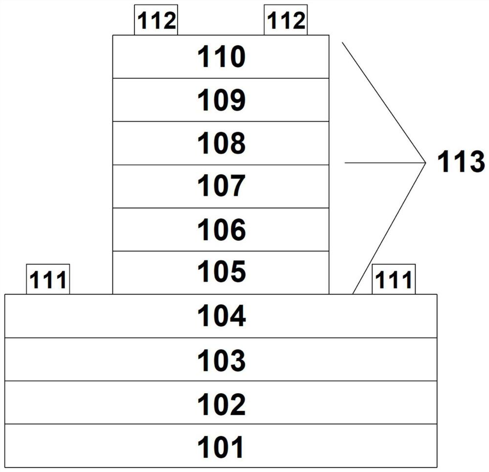
[0030] Such as figure 1 As shown, Embodiment 1 is a schematic structural diagram of a bipolar visible light detector based on Group III nitride semiconductors. The device structure is grown by metal-organic chemical vapor deposition or molecular beam epitaxy, including a c-plane sapphire substrate 101 and an epitaxial layer grown on the substrate 101 . Among them, the order of the epitaxial layer from bottom to top is a 25nm thick low temperature GaN nucleation layer 102, a 3μm thick high temperature unintentionally doped GaN transition layer 103, a 2μm thick electron concentration of 3×10 18 cm -3 The Si-doped n-type GaN lower ohmic contact layer 104 has a thickness of 100 nm and an electron concentration of 3×10 18 cm -3 Al x Ga 1-x N (x start value is 0, end value is 0.15) composition graded layer 105, 5nm thick Al y Ga 1-y N (y=0.15) unintentionally doped layer 106, 110nm thick unintentionally doped Al z Ga 1-z N (start value of z is 0.1, end value is 0) compositi...

Embodiment 2

[0032] This embodiment 2 is a preparation method of a bipolar visible light detector, which specifically includes the following steps:

[0033] S1. Surface cleaning: Place the wafer in acetone and isopropanol in turn, and perform organic cleaning by ultrasonic vibration. After cleaning with deionized water, place the wafer in 50% hydrochloric acid solution to remove the surface oxide layer , blow dry with a pure nitrogen gun;

[0034] S2. Step production: apply glue, photolithography, and develop to expose the part that needs to be etched, and then use inductively coupled plasma to dry etch the wafer to the ohmic contact layer 104 under the Si-doped n-type GaN, and use a glue remover to glue;

[0035] S3. Etching damage repair: treat the wafer with boiled KOH solution, and then use it in high-purity N 2 The rapid thermal annealing process under the atmosphere is annealed at 700 ° C for 1 min;

[0036] S4. Electrode production: glue coating, photolithography, and development...


PUM

PropertyMeasurementUnit
thicknessaaaaaaaaaa
thicknessaaaaaaaaaa
thicknessaaaaaaaaaa

Abstract

The invention relates to a bipolar visible light detector and a preparation method thereof. The bipolar visible light detector includes a substrate, an epitaxial layer, and a deposited metal electrode. The epitaxial layer is sequentially grown from bottom to top as a nucleation layer, Transition layer, Si-doped n-type GaN lower ohmic contact layer, Si-doped n-type Al x Ga 1‑x Gradient layer of N composition, unintentional doping of Al y Ga 1‑y N layer, unintentionally doped Al z Ga 1‑z N-composition graded layer, unintentionally doped In with periodic GaN thin insertion layer j Ga 1‑j N light absorbing layer, Si doped n-type In k Ga 1‑k The N composition gradient layer, the Si-doped n-type GaN upper ohmic contact layer, and the metal electrodes include a lower ohmic contact electrode and an upper ohmic contact electrode. The invention has the advantages of high photoelectric gain, fast response speed and low working voltage.

Description

technical field [0001] The present invention relates to the technical field of semiconductor visible light detectors, in particular to a bipolar visible light detector and a preparation method thereof. Background technique [0002] At present, applications in the fields of visible light communication, biophotonics, and fluorescence spectroscopy have put forward higher requirements on the performance of visible light detectors. Group III nitride semiconductor InGaN ternary alloys, due to the direct and tunable bandgap energy from 0.7 to 3.4eV covering the entire visible region by changing the composition of indium (In), have promising applications in visible light detection ; At the same time, because InGaN is a direct bandgap semiconductor, and has the material characteristics of high light absorption coefficient and fast electron saturation drift speed, it is a highly efficient and high-speed visible light detector material with great potential. [0003] To date, various t...

Claims


Application Information

Patent Timeline
Patent Type & Authority Patents(China)
IPC IPC(8): H01L31/0304H01L31/102H01L31/18G01J1/44
CPCG01J1/44G01J2001/4446H01L31/03044H01L31/03048H01L31/102H01L31/1848H01L31/1852H01L31/1856Y02P70/50
Inventor 江灏张苏朋吕泽升
Owner SUN YAT SEN UNIV
Why Eureka
Try Eureka