
Processing technology of invisible fingerprint film layer

A processing technology and invisible fingerprint technology, which is applied in the processing technology field of vapor-depositing an invisible fingerprint film layer on a glass cover, can solve the problem of affecting product quality, optimizing customer experience, interfering with glass refractive index and reflectivity, and reducing glass optical performance. and other issues, to achieve the effect of improving processing yield, shortening coating time, and improving bonding force

Inactive Publication Date: 2020-07-03
LENS TECH CHANGSHA
View PDF5 Cites 2 Cited by
  • Summary
  • Abstract
  • Description
  • Claims
  • Application Information

AI Technical Summary

Problems solved by technology

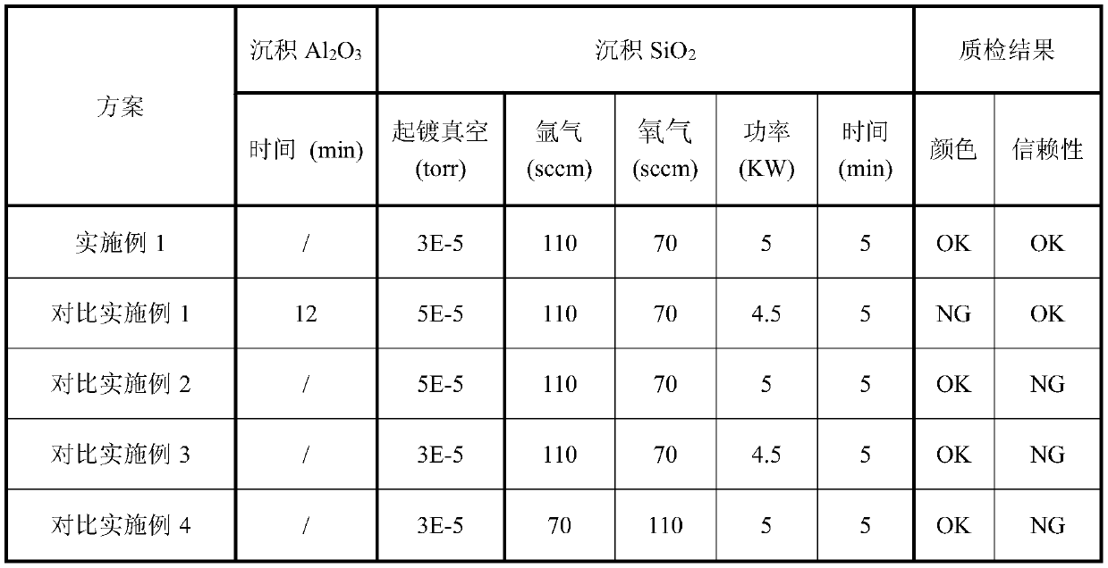
[0005] 1. Due to the need to sequentially sputter deposition between the glass surface and the IF film to form Al 2 o 3 layer and SiO 2 layer, so the process increases, the processing time is prolonged, and the processing efficiency is reduced;
[0006] 2. Due to the formation of Al in the process of IF film processing 2 o 3 layer, while Al 2 o 3 Improper deposition process of the layer can lead to Al 2 o 3 layer appears red in the visible spectrum, while the Al 2 o 3 with SiO 2 Due to the interference effect of the film in the visible spectrum range, the glass will reflect red light. The above-mentioned redness problem on the glass surface will reduce the optical performance of the glass, interfere with the refractive index and reflectivity of the glass, and seriously affect Improvement of product quality and optimization of customer experience

Method used


Image

  • Processing technology of invisible fingerprint film layer

Examples


Embodiment 1

[0027] A process for processing an invisible fingerprint film layer, in which an IF film is coated on the surface of aluminosilicate glass, the specific process is as follows:

[0028] Step 1) Ion source cleaning: place the jig carrying the glass product to be coated in the vacuum chamber, evacuate the chamber to 8E-5torr, and generate plasma with a voltage of 790V to bombard the glass surface under the condition of argon gas flow rate of 1000sccm. Realize the cleaning of the glass surface, the cleaning time is 300s;

[0029] Step 2) Sputter deposition of SiO 2 : Evacuate the vacuum in the cavity to 3E-5torr, under the conditions of argon flow rate of 110sccm and oxygen flow rate of 70sccm, the silicon molecules in the silicon target are sputtered out with a sputtering power of 5000W, and the silicon molecules react with oxygen Form SiO 2 and deposited on the glass surface to form SiO 2 layer;

[0030] Step 3) evaporative deposition of IF: the IF film material is heated in...


PUM


Abstract

The invention provides a processing technology of an invisible fingerprint film layer. The processing technology comprises the steps of first, putting glass in a cavity of a coating machine, conducting vacuumizing until the vacuum degree is 8E-5 torr, introducing argon with the flow of 1000 sccm, and generating plasma with radio-frequency voltage of 790 V to bombard the surface of the glass for 300 s so as to clean the surface of the glass; then continuing to lower the vacuum degree to 3E-5 torr, introducing argon with the flow of 110 sccm and oxygen with the flow of 70 sccm, sputtering silicon molecules in a silicon target with the sputtering power of 5000 W, carrying out a reaction between the silicon molecules and oxygen to produce SiO2, and depositing SiO2 on the surface of the glass;and finally, adopting steam resistance for heating IF film, setting voltage and current to be 2.5 V and 860 A respectively to conduct evaporation for 400 s, and depositing the IF film on the SiO2 layer after evaporation. By means of the processing technology of the invisible fingerprint film layer, the coating time is shortened, the production cost is lowered, the problem that the surface of the glass goes red is solved, and reliability requirements of the product are met at the same time.

Description

technical field [0001] The invention relates to the technical field of glass cover production, in particular to a processing technology for vapor-depositing an invisible fingerprint film layer on a glass cover. Background technique [0002] Invisible fingerprint film, that is, IF (Invisible Fingerprint) film is mainly used on the surface of the glass cover of mobile phone. Oil stains and sweat stains on the fingers remain on the glass surface to form fingerprints. Due to the hydrophobic and lipophilic properties of the IF film, it can dissolve and diffuse grease stains, effectively dilute the visibility of grease traces, and make the outline of fingerprints less obvious. Invisible effect on glass surfaces. [0003] The existing IF film processing process is as follows: aluminosilicate glass is used as the substrate, this type of glass is mainly composed of Al 2 o 3 and SiO 2 Composition, the glass surface is firstly cleaned by plasma, and then Al is deposited on the glas...

Claims


Application Information

Patent Timeline
Patent Type & Authority Applications(China)
IPC IPC(8): C23C14/34C23C14/10C23C14/26C23C14/02
CPCC23C14/022C23C14/10C23C14/26C23C14/34
Inventor 宋志伟何有斌
Owner LENS TECH CHANGSHA
Learn More