Surface metallization method for composite dielectric substrate of printed circuit

A composite medium and substrate surface technology, which is applied in the direction of printed circuit, improvement of metal adhesion of insulating substrate, printed circuit manufacturing, etc., can solve problems such as missing plating, plating layer falling off, etc., to speed up deposition, increase surface roughness, enhance The effect of binding strength

Pending Publication Date: 2020-06-26
UNIV OF ELECTRONICS SCI & TECH OF CHINA
View PDF8 Cites 1 Cited by
  • Summary
  • Abstract
  • Description
  • Claims
  • Application Information

AI Technical Summary

Problems solved by technology

[0004] The object of the present invention is to propose a method for surface metallization of a printed circuit composite dielectric substrate in view of problems such as anti-plating, missing plating, and coating shedding that exist in the existing printed circuit composite dielectric substrate surface metallization in the background technology. The metal coating obtained by this method has good bonding strength with the composite dielectric substrate

Method used


Image

  • Surface metallization method for composite dielectric substrate of printed circuit
  • Surface metallization method for composite dielectric substrate of printed circuit
  • Surface metallization method for composite dielectric substrate of printed circuit

Examples


Embodiment

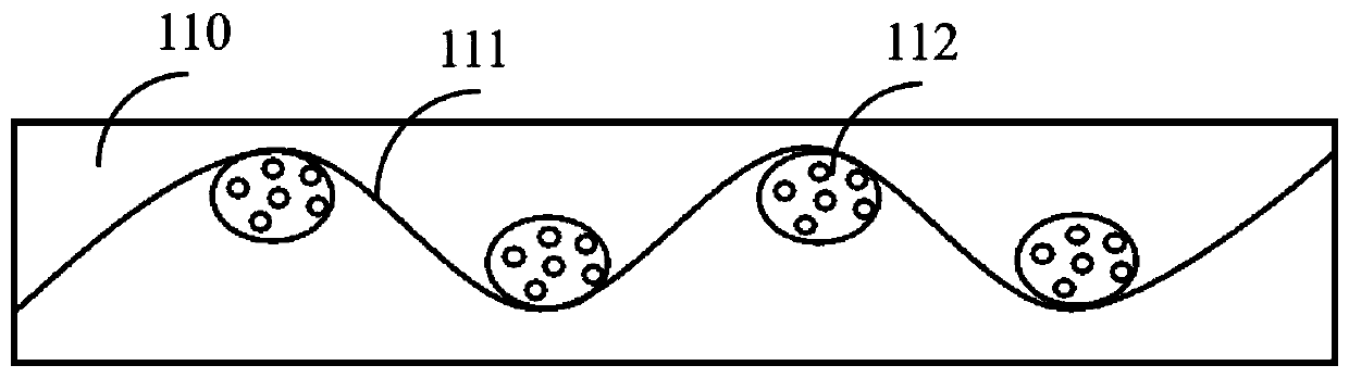
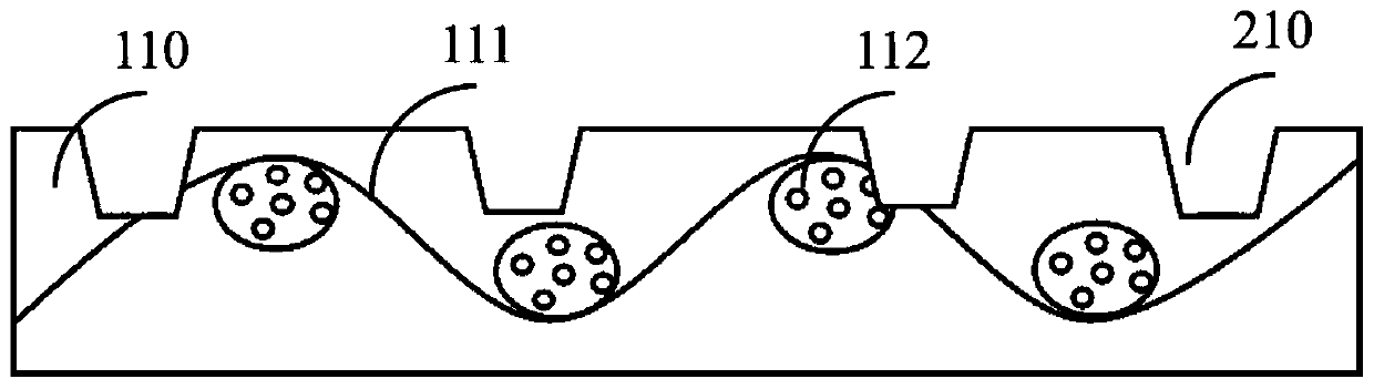
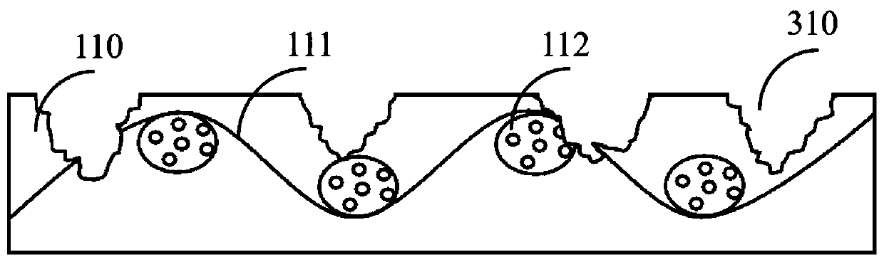
[0038] Step 1. Form a plurality of densely packed holes (210) with a depth of 2 μm and a diameter of 100 μm arranged in an array on the surface of the carbon fiber / cyanate composite dielectric substrate by laser drilling, wherein the spacing between adjacent holes is 80 μm. The laser energy is 0.4mJ, and the pulse width is 2μs; the 2D and 3D roughness images of the carbon fiber / cyanate composite dielectric substrate exposed resin and fiber cloth after laser ablation in step 1 are as follows Figure 6 As shown in (c) and 6(d), it shows that laser ablation forms dense holes on the surface of the dielectric substrate, which increases the surface roughness and is conducive to the formation of a riveting structure between the metal coating and the dielectric substrate;

[0039] Step 2, performing low-temperature plasma roughening on the composite dielectric substrate treated in step 1, specifically: placing the composite dielectric substrate at 80% O 2 and 20% CF 4 (volume percent...


PUM

PropertyMeasurementUnit
depthaaaaaaaaaa
pore sizeaaaaaaaaaa

Abstract

A surface metallization method for a composite dielectric substrate of a printed circuit belongs to the technical field of printed circuit board manufacturing. The method comprises the following steps: (1) forming holes with the depth of 1-2 [mu]m in the surface of a composite dielectric substrate of a printed circuit by adopting a laser drilling method; (2) sequentially adopting a low-temperatureplasma method and a potassium permanganate method to carry out surface etching treatment on the dielectric substrate treated in the previous step; (3) chemically plating a copper seed layer; and (4)electroplating copper to realize surface metallization of the composite dielectric substrate of the printed circuit. According to the surface metallization method for a composite dielectric substrateof a printed circuit provided by the invention, before roughening treatment, a laser drilling method is adopted to selectively ablate the composite dielectric substrate to form dense holes and exposeresin and fiber cloth, on one hand, the surface roughness of the composite dielectric substrate is increased, and on the other hand, the dense holes enable a riveting structure to be formed between ametal plating layer and the dielectric substrate, and the bonding strength between the plating layer and the dielectric substrate is enhanced.

Description

technical field [0001] The invention belongs to the technical field of printed circuit board production, and in particular relates to a method for metallizing the surface of a printed circuit composite dielectric substrate. Background technique [0002] The printed circuit composite dielectric substrate has become an excellent material for the production of high-frequency, high-speed, high-performance printed circuits due to its excellent thermal stability, dielectric properties, mechanical properties, adhesion, and good processing technology. Widely used in communication equipment, automotive electronics, consumer electronics, aviation defense and other fields. However, due to the low surface energy and roughness of the printed circuit composite dielectric substrate, direct surface metallization will weaken the bonding strength between the composite dielectric substrate and the metal coating, causing problems such as coating peeling and missing plating, which seriously hind...

Claims


Application Information

Patent Timeline
Patent Type & Authority Applications(China)
IPC IPC(8): H05K3/02H05K3/38
CPCH05K3/022H05K3/381
Inventor 游相清何为曹金东叶之洋孙弘毅陈苑明王守绪王翀周国云洪延杨文君
Owner UNIV OF ELECTRONICS SCI & TECH OF CHINA
Why Eureka
Try Eureka