Flexible all-carbon resistive random access memory and preparation method thereof
A resistive memory and flexible technology, applied in electrical components and other directions, can solve the problems of limiting the development and application of memory devices, and difficult to meet the needs of large data storage, and achieve the effects of good cycle stability, stable cycle scanning, and low misread rate.
- Summary
- Abstract
- Description
- Claims
- Application Information
AI Technical Summary
Problems solved by technology
Method used
Image

Examples
Embodiment 1
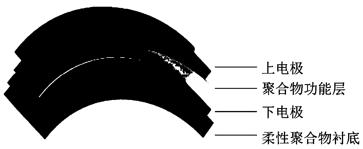
[0051] Such as figure 1 As shown, the structure of a flexible all-carbon nonvolatile memory is a sandwich structure, which has an upper electrode, a lower electrode and a middle active layer. The memory adopts rGO as the upper and lower electrodes, the middle resistive switching functional layer is a polymer semiconductor material, and the middle active layer is formed on the surface of the lower electrode by spin coating.
[0052] (1) Substrate treatment: Sonicate the silicon dioxide / silicon wafer substrate with ethanol, isopropanol, and deionized water for 10 minutes, blow dry with nitrogen, and then treat it with an oxygen plasma cleaner at a power of 50W for 3 minutes.
[0053] (2) Flexible substrate treatment: Ultrasonic the ethylene glycol diformate plastic with ethanol, isopropanol, and deionized water for 10 min, respectively, and blow dry with nitrogen.
[0054](3) Preparation of lower electrode: Spin-coat graphene oxide solution on silicon dioxide / silicon wafer subs...
Embodiment 2
[0059] A method for preparing a flexible all-carbon nonvolatile memory, comprising the following steps:
[0060] (1) Substrate treatment: Sonicate the silicon dioxide / silicon wafer substrate with ethanol, isopropanol, and deionized water for 12 minutes, blow dry with nitrogen, and then treat it with an oxygen plasma cleaner at a power of 25W for 5 minutes.
[0061] (2) Flexible substrate treatment: Sonicate the polyethersulfone resin with ethanol, isopropanol, and deionized water for 12 minutes, respectively, and blow dry with nitrogen.
[0062] (3) Preparation of the lower electrode: first spin-coat the graphene oxide solution on the silicon dioxide / silicon wafer substrate to obtain a large-area graphene oxide film, and then mix it under argon / hydrogen gas (volume ratio of 95 / 5) Reducing at a high temperature of 1100° C. for 1.5 hours in an atmosphere to obtain a reduced graphene oxide film. Subsequent exfoliation in NaOH solution yielded self-supporting rGO films. The rGO ...
Embodiment 3
[0067] A method for preparing a flexible all-carbon nonvolatile memory, comprising the following steps:
[0068] (1) Substrate treatment: Sonicate the silicon dioxide / silicon wafer substrate with ethanol, isopropanol, and deionized water for 15 minutes, blow dry with nitrogen, and then treat it with an oxygen plasma cleaner at a power of 10W for 8 minutes.
[0069] (2) Flexible substrate treatment: the polyimide was ultrasonicated for 15 min with ethanol, isopropanol, and deionized water respectively, and dried with nitrogen gas.
[0070] (3) Preparation of the lower electrode: first spin-coat the graphene oxide solution on the silicon dioxide / silicon wafer substrate to obtain a large-area graphene oxide film, and then mix it under argon / hydrogen gas (volume ratio of 95 / 5) Reducing at a high temperature of 1200° C. for 0.5 hour in an atmosphere to obtain a reduced graphene oxide film. Subsequent exfoliation in NaOH solution yielded self-supporting rGO films. Flexible rGO ele...
PUM
| Property | Measurement | Unit |
|---|---|---|
| Thickness | aaaaa | aaaaa |
| Weight average molecular weight | aaaaa | aaaaa |
| Number average molecular weight | aaaaa | aaaaa |
Abstract
Description
Claims
Application Information
 - Generate Ideas
- Intellectual Property
- Life Sciences
- Materials
- Tech Scout
- Unparalleled Data Quality
- Higher Quality Content
- 60% Fewer Hallucinations
Browse by: Latest US Patents, China's latest patents, Technical Efficacy Thesaurus, Application Domain, Technology Topic, Popular Technical Reports.
© 2025 PatSnap. All rights reserved.Legal|Privacy policy|Modern Slavery Act Transparency Statement|Sitemap|About US| Contact US: help@patsnap.com