Pretreatment method of TSV blind hole electro-coppering hard warped wafer before chemical mechanical polishing

A chemical mechanical and electroplating copper technology, which is applied in the direction of circuits, electrical components, electric solid devices, etc., can solve the problems of automatic feeding of equipment, poor polishing uniformity, uncontrollable direction, etc., so as to avoid automatic feeding of equipment and realize The effect of global flattening and reducing the thickness of the glue layer

Inactive Publication Date: 2020-06-19
XIAN MICROELECTRONICS TECH INST
View PDF6 Cites 0 Cited by
  • Summary
  • Abstract
  • Description
  • Claims
  • Application Information

AI Technical Summary

Problems solved by technology

[0003] In the CVD process, PVD process and blind via copper plating process, the stress is often generated due to the dielectric layer of different thickness deposited or plated on the surface, resulting in different degrees of hard warping of the wafer
In addition, because in the copper plating process of blind vias, the current tends to gather at the place where the fixture contacts the edge of the wafer, forming irregular copper bumps or copper bumps, resulting in the uniform thickness of the copper layer on the entire surface of the TSV blind via plating wafer. poor sex
[0004] Due to the varying size and uncontrollable direction of the hard warpage of the wafer, it is impossible to ensure that the process surface of the wafer is in full contact with the polishing pad during chemical mechanical polishing (abbreviated as CMP). After polishing, poor polishing uniformity and localized Severe over-polishing phenomenon. If the wafer warpage is too large, there may even be problems such as automatic loading of the equipment, wafer cracks, excessive leakage current, and abnormal damage or loss of the polishing pad.

Method used


Image

  • Pretreatment method of TSV blind hole electro-coppering hard warped wafer before chemical mechanical polishing
  • Pretreatment method of TSV blind hole electro-coppering hard warped wafer before chemical mechanical polishing
  • Pretreatment method of TSV blind hole electro-coppering hard warped wafer before chemical mechanical polishing

Examples


Embodiment Construction

[0030] The present invention will be further described in detail below in conjunction with specific embodiments, which are explanations of the present invention rather than limitations.

[0031] The pretreatment method before chemical mechanical polishing of TSV blind hole electroplating copper hard warping wafer of the present invention comprises the following steps,

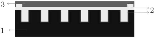
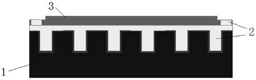
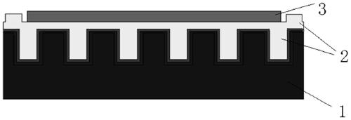
[0032] Step 1. Spray a layer of positive photoresist or negative photoresist on the graphics surface of the TSV copper-plated hard-warped wafer to completely cover the electroplated surface copper, copper bumps or copper bumps ;

[0033] Step 2: Cover the central position of the wafer with a matching mask to leak out the edge area; perform directional exposure on the leaked area at the edge of the wafer through an exposure machine; use a developing solution to expose the hard warped edge area of ​​the TSV blind hole electroplating copper Perform development to remove the photoresist in this area, exposing the ...


PUM

PropertyMeasurementUnit
thicknessaaaaaaaaaa

Abstract

The invention provides a pretreatment method for a TSV blind hole electro-coppering hard warped wafer before chemical mechanical polishing. The method comprises the following steps: step 1, spraying alayer of photoresist on the pattern surface of a TSV blind hole electrocoppering hard warping wafer, then shielding the central position of the wafer and then carrying out directional exposure, taking an unexposed area of the wafer as an edge area, and finally removing the photoresist in the edge area of the wafer; step 2, the wafer obtained in the step 1 is subjected to photoresist removing treatment and then soaked in corrosive liquid, and a wafer with surface copper and copper protruding points or copper protruding blocks removed is obtained; and 3, removing the photoresist on the patternsurface of the wafer obtained in the step 2, and thinning the back surface of the obtained wafer to finish the pretreatment of the TSV blind hole electro-coppering hard warped wafer before chemical mechanical polishing. Hard warping of the wafer is converted into soft warping so that complete contact between the wafer and the polishing pad is easier to realize and global planarization is realized.

Description

technical field [0001] The invention belongs to the cross technical field of semiconductor and advanced packaging, in particular to a pretreatment method before chemical mechanical polishing of TSV blind hole electroplating copper hard warping wafer. Background technique [0002] In the semiconductor TSV (English full name: Through Silicon Via) interconnection process, in order to meet the conduction requirements of the device, it is necessary to fill the through-silicon vias through the blind via copper plating process to realize the electrical interconnection between the front and back of the chip. In the semiconductor TSV interconnection process, the completion of through-silicon via etching requires the preparation of the barrier layer and the seed layer through the CVD process and the PVD process in sequence, and then through the blind hole electroplating copper process to make the metal copper slowly along the seed layer in the hole wall. Deposit until the copper pilla...

Claims


Application Information

Patent Timeline
Patent Type & Authority Applications(China)
IPC IPC(8): H01L21/768
CPCH01L21/7684H01L2221/1068
Inventor 岳永豪吴道伟刘建军牛昊梅志鹏
Owner XIAN MICROELECTRONICS TECH INST
Why Eureka
Try Eureka