Array substrate manufacturing method, array substrate and liquid crystal display device
A technology of an array substrate and a manufacturing method, which is applied in the field of display, can solve problems affecting display effects, etc., and achieve the effect of improving transmittance and transmittance
- Summary
- Abstract
- Description
- Claims
- Application Information
AI Technical Summary
Problems solved by technology
Method used
Image

Examples
Embodiment 1
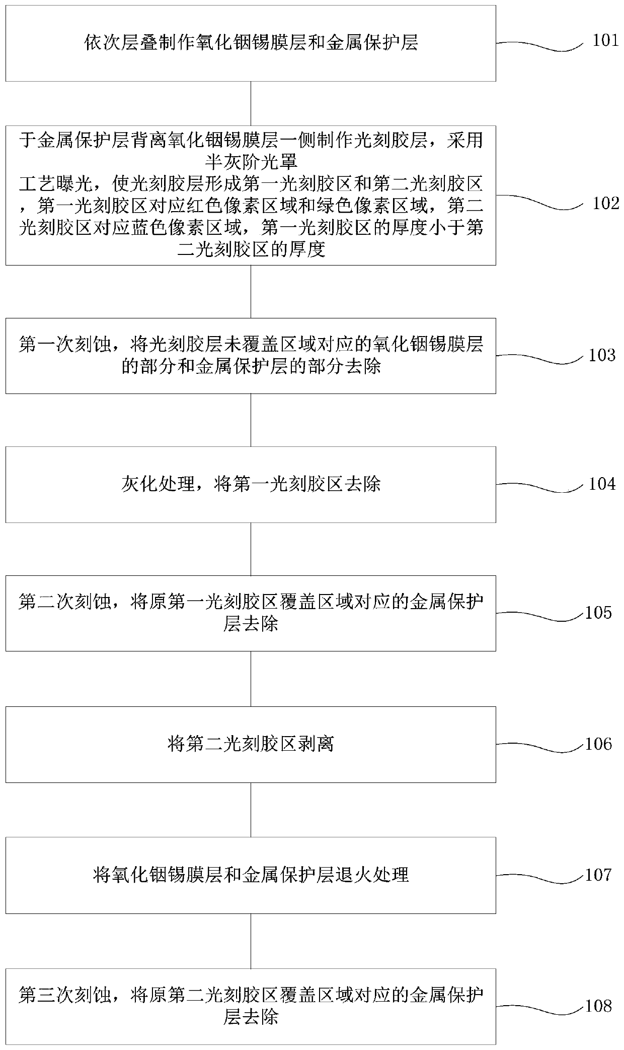
[0046] Such as figure 1As shown, a method for manufacturing an array substrate proposed in Embodiment 1 of the present invention includes manufacturing a gate layer, a gate insulating layer, an active layer, a source / drain layer, a passivation insulating layer, a first an indium tin oxide film layer and a second indium tin oxide film layer.
[0047] Specifically, the gate layer, the gate insulating layer, the active layer, the source / drain layer, the passivation insulating layer, the first indium tin oxide film layer and the second indium tin oxide film layer, the specific composition of these film layers, The thickness and the manufacturing process are conventional means, and will not be repeated here. Gate layer, gate insulation layer, active layer, source / drain layer, passivation insulation layer, first indium tin oxide film layer and second indium tin oxide film layer, the successive stacking of these film layers on the substrate The order can be specifically set accordi...
Embodiment 2
[0076] An array substrate proposed in Embodiment 2 of the present invention includes:
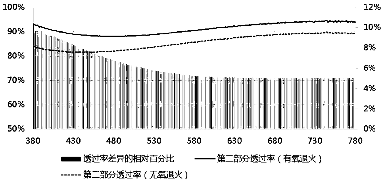
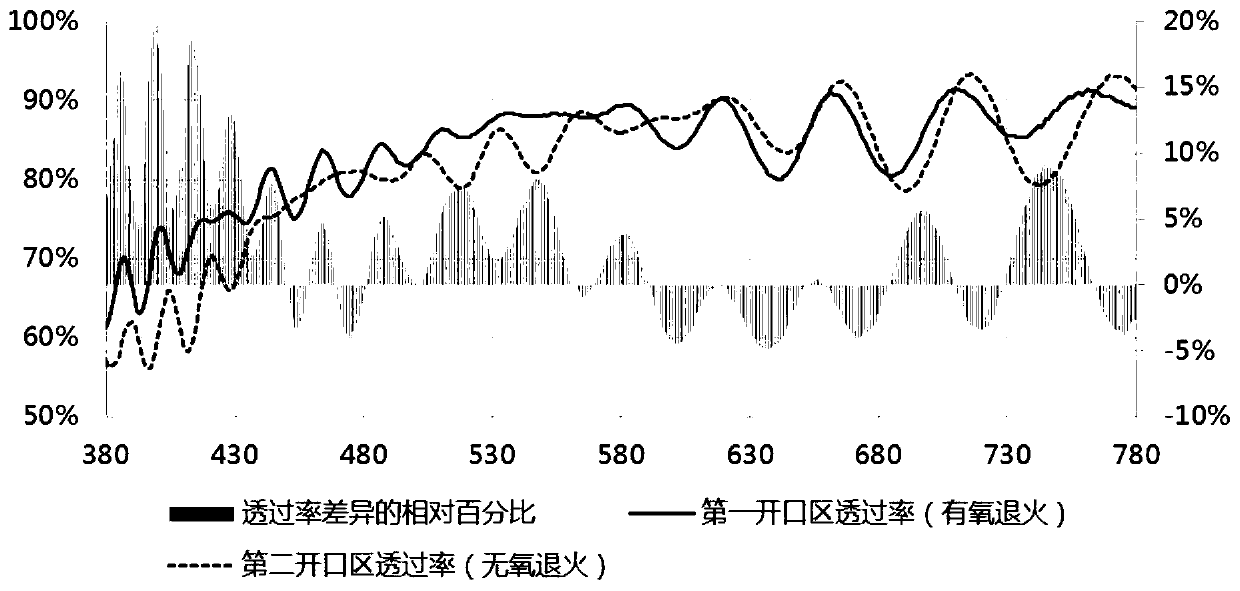
[0077] A glass substrate, a first indium tin oxide film layer, and a second indium tin oxide film layer, the first indium tin oxide film layer is closer to the glass substrate than the second indium tin oxide film layer; wherein, the first The part of the indium tin oxide film layer corresponding to the red pixel area and the green pixel area is the first opening area, and the part of the first indium tin oxide film layer corresponding to the blue pixel area is the second opening area, such as image 3 As shown, the transmittance of the second opening area in the 380nm-450nm light band is lower than the transmittance of the first opening area.
[0078] For example, the specific structure of the array substrate proposed in Embodiment 2 may be:
[0079] 1. A gate layer, a gate insulating layer, an active layer, a source / drain layer, a passivation insulating layer, and a second indium tin oxi...
Embodiment 3
[0086] A liquid crystal display device proposed in Embodiment 3 of the present invention, which includes: an array substrate;
[0087] The array substrate includes: a glass substrate, a first indium tin oxide film layer and a second indium tin oxide film layer, the first indium tin oxide film layer is closer to the glass substrate than the second indium tin oxide film layer ; Wherein, the part of the first indium tin oxide film layer corresponding to the red pixel area and the green pixel area is the first opening area, and the part of the first indium tin oxide film layer corresponding to the blue pixel area is the second opening area, the transmittance of the second opening area in the 380nm-450nm light band is lower than the transmittance of the first opening area.
[0088] Specifically, the array substrates used in the three embodiments of the present invention can directly use the array substrates in the second embodiment, which will not be repeated here.
[0089] In the...
PUM
 Abstract
Description
Claims
Application Information
 - R&D
- Intellectual Property
- Life Sciences
- Materials
- Tech Scout
- Unparalleled Data Quality
- Higher Quality Content
- 60% Fewer Hallucinations
Browse by: Latest US Patents, China's latest patents, Technical Efficacy Thesaurus, Application Domain, Technology Topic, Popular Technical Reports.
© 2025 PatSnap. All rights reserved.Legal|Privacy policy|Modern Slavery Act Transparency Statement|Sitemap|About US| Contact US: help@patsnap.com