Microwave power amplifier chip carrier and preparation method thereof

A power amplifier chip and carrier technology, which is applied in the direction of electric solid-state devices, semiconductor devices, semiconductor/solid-state device components, etc., can solve the problems of increasing the manufacturing process steps of T/R components, polluting microwave power chips, etc., to meet the requirements of high-efficiency heat dissipation and Low thermal stress requirements, reduced manufacturing processes, and improved reliability

Active Publication Date: 2020-05-12
SHANGHAI SPACEFLIGHT ELECTRONICS & COMM EQUIP RES INST
View PDF7 Cites 4 Cited by
  • Summary
  • Abstract
  • Description
  • Claims
  • Application Information

AI Technical Summary

Problems solved by technology

This not only increases the manufacturing process steps of T / R components, but also has the risk of solder or glue overflowing under the chip capacitor to contaminate the microwave power chip

Method used


Image

  • Microwave power amplifier chip carrier and preparation method thereof
  • Microwave power amplifier chip carrier and preparation method thereof
  • Microwave power amplifier chip carrier and preparation method thereof

Examples


Embodiment 1

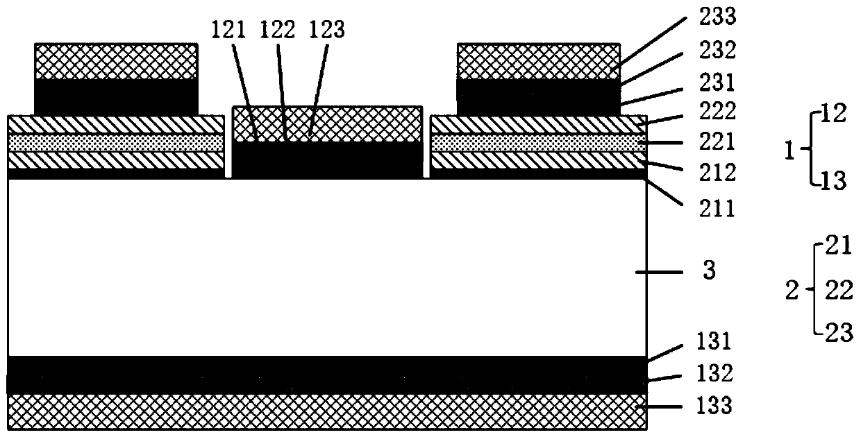
[0044] see figure 1 The microwave power amplifier chip carrier of this embodiment includes: a high-silicon aluminum alloy substrate 3, a chip spacer 1, and a film capacitor 2. The high-silicon aluminum alloy substrate 3 has two parallel planes, which are respectively the first surface and the second surface , the silicon content of the high-silicon aluminum alloy substrate 3 is preferably more than 25%, and its first surface roughness is less than 100 nm, and its second surface roughness is less than 1 μm;

[0045] The chip pad 1 includes a chip bonding metal layer 12 and a carrier bonding metal layer 13. The chip bonding metal layer 12 is formed on the power chip bonding area on the first surface of the high-silicon aluminum alloy substrate 3, and the carrier bonding metal layer 13 is formed on the high-silicon aluminum alloy substrate 3. The second surface of the substrate 3; the die bonding metal layer 12 includes a second metal seed layer 121, a second barrier layer 122 an...

Embodiment 2

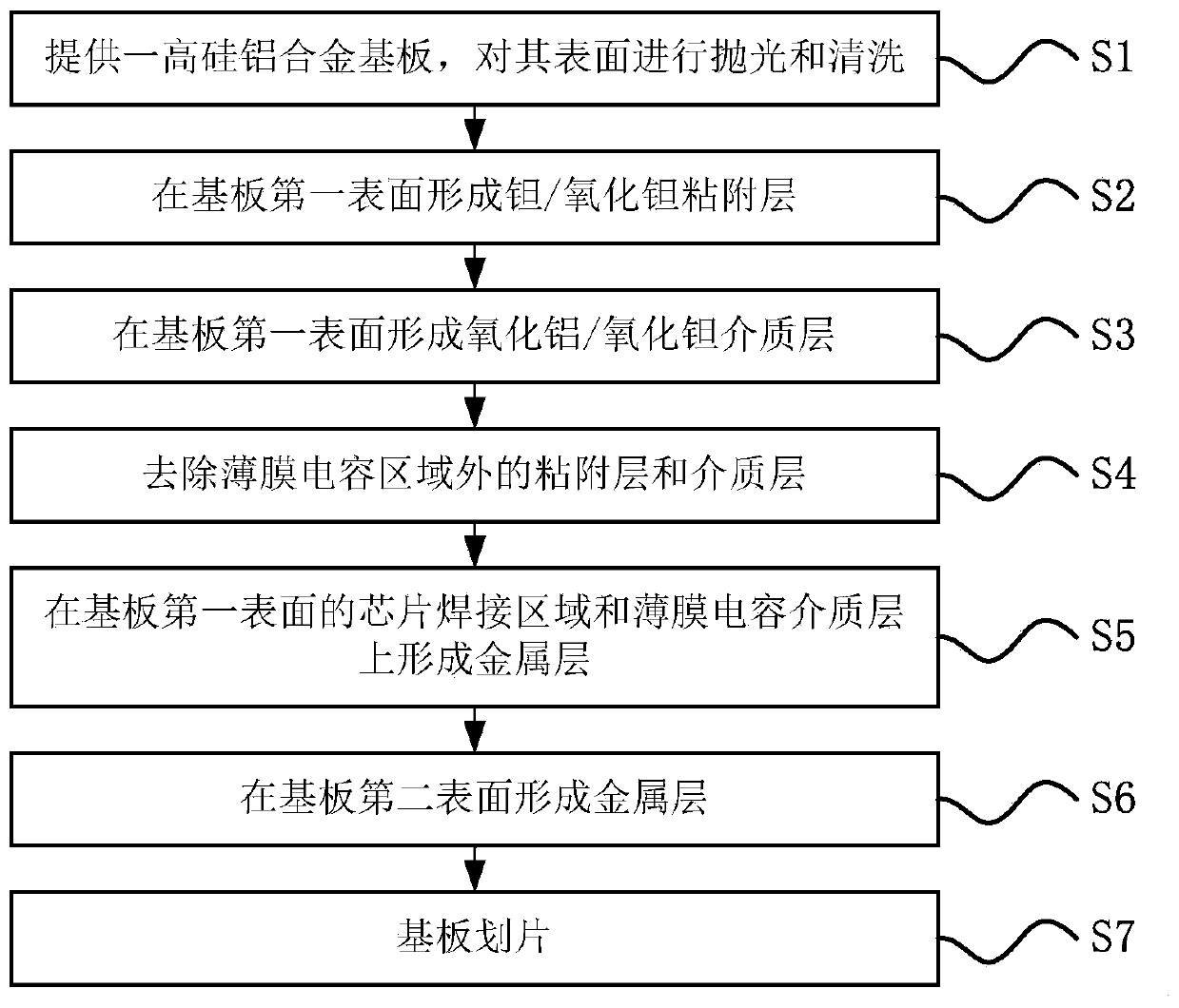
[0052] refer to Figure 2-Figure 9 , this embodiment provides a method for preparing the microwave power amplifier chip carrier provided by Embodiment 1. This embodiment is based on the selection of the same metal for the wire bonding layer 233 and the first soldering layer 123. The specific steps of the method are as follows :

[0053] S1: see image 3 , performing chemical mechanical polishing and cleaning on the first surface and the second surface of the high-silicon aluminum alloy substrate 3, so that the roughness of the first surface is lower than 100 nm, the roughness of the second surface is lower than 1 μm, and the first surface and the second surface are two surfaces of the high-silicon aluminum alloy substrate 3 parallel to each other;

[0054] S2: see Figure 4 , using magnetron sputtering technology, sequentially sputtering tantalum film 211 and tantalum oxide film 212 on the first surface of the high-silicon aluminum alloy aluminum substrate to form an adhesi...

Embodiment 3

[0062] The difference from Example 2 is that in steps S2 to S4, the adhesive layer 21 and the dielectric layer 22 of the thin film capacitor 2 are prepared by using the lift-off process, specifically, glue is first applied on the first surface and the thin film capacitor 2 is pre-embedded by photolithography. For the window, the thin film capacitor 2 is deposited on the first surface of the window pattern on which the thin film capacitor 2 is pre-buried, and then the film in the non-film capacitor 2 area is peeled off by glue removal.


PUM

PropertyMeasurementUnit
surface roughnessaaaaaaaaaa

Abstract

The invention discloses a microwave power amplifier chip carrier and a preparation method thereof. The microwave power amplifier chip carrier comprises a high silicon aluminum alloy substrate, a chipcushion block and a film capacitor; the chip cushion block comprises a chip welding metal layer and a carrier welding metal layer, and the film capacitor comprises a bonding layer, a dielectric layerand an electrode metal layer. The manufacturing method comprises the following steps: providing the high silicon aluminum alloy substrate with a polished surface, and sequentially forming the bondinglayer and the dielectric layer in a thin film capacitor region on the first surface of the substrate; forming the metal layer on the chip welding area on the first surface of the substrate and the surface of the thin-film capacitor dielectric layer; after a carrier welding metal layer is formed on the second surface of the substrate, performing scribing. According to the microwave power amplifierchip carrier and the manufacturing method provided by the invention, the microwave power amplifier chip cushion block and the chip capacitor are integrated into a whole, the manufacturing process steps of a microwave assembly can be effectively reduced, the process difficulty is reduced, and in addition, the chip carrier also has excellent heat dissipation performances, grounding performances andreliability.

Description

technical field [0001] The invention belongs to the field of microwave component parts manufacturing and micro-assembly, and in particular relates to a microwave power amplifier chip carrier and a preparation method thereof. Background technique [0002] The active phased array radar with T / R components as the core has the advantages of fast scanning, digital beam forming and space power combining, and can simultaneously complete multiple functions such as early warning, tracking guidance and fire control, and has a very strong multi-target processing capability , is the advanced equipment that the modern combat system relies on. [0003] At present, most T / R components are manufactured using multi-chip component technology, and the microwave power amplifier chip is one of the key chips inside the T / R component, which has high requirements for heat dissipation, grounding performance and reliability. In order to meet the above requirements, the mature process scheme is to us...

Claims


Application Information

Patent Timeline
Patent Type & Authority Applications(China)
IPC IPC(8): H01L23/14H01L23/36H01L23/373H01L23/64
CPCH01L23/14H01L23/36H01L23/3736H01L23/642
Inventor 刘米丰丁蕾王立春任卫朋周义
Owner SHANGHAI SPACEFLIGHT ELECTRONICS & COMM EQUIP RES INST
Why Eureka
Try Eureka