Preparation process of solar cell
A solar cell and preparation process technology, applied in the field of solar cells, can solve the problems of affecting solar cell current, serious absorption, etc., and achieve the effects of improving photoelectric conversion efficiency, improving minority carrier life, and reducing metal-semiconductor contact with minority carrier recombination
- Summary
- Abstract
- Description
- Claims
- Application Information
AI Technical Summary
Problems solved by technology
Method used
Image


Examples
preparation example Construction
[0080] In the preparation process of the above-mentioned solar cell:
[0081] Preferably, the silicon substrate in step S1 is a P-type silicon wafer.
[0082] Before the silicon substrate 1 is provided with a doped silicon layer, the silicon substrate 1 is textured and a P-N junction 2 is formed. The P-N junction 2 can be formed by means of thermal diffusion, ion implantation and annealing. For P-type silicon wafers, the diffusion is phosphorus diffusion.
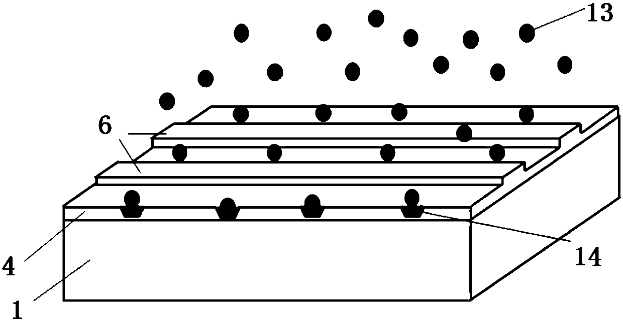
[0083] After the P-N junction 2 is made, the back of the silicon substrate is leveled, and the phosphosilicate glass on the front of the silicon substrate is removed, and then a tunneling passivation layer 3 is provided on at least one surface of the diffused silicon substrate.
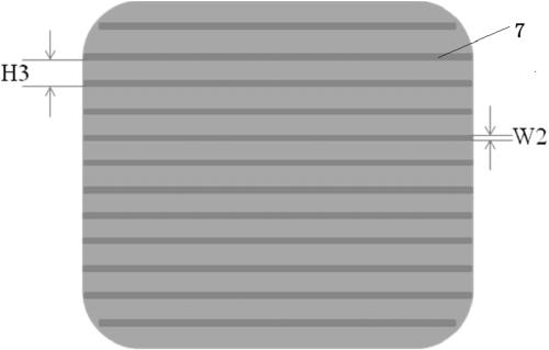
[0084] Preferably, a tunneling passivation layer 3 is provided on at least one surface of the diffused silicon substrate, and then an intrinsic silicon layer 4 is provided on the tunneling passivation layer 3, and the intrinsic silicon layer 4 ca...
Embodiment 1
[0109] This embodiment provides a PERC cell with a local Topcon contact structure on the light-receiving surface. In this solar cell, a local doped silicon structure is arranged on the light-receiving surface of the PERC cell. The preparation steps are as follows:
[0110] A. Surface texturing: Provide silicon substrate 1, choose P-type monocrystalline silicon wafer for silicon substrate 1, its volume resistivity is 2.0Ω·cm, complete the surface texturing of silicon wafer, and the surface reflectance of single crystal silicon wafer is 13%;
[0111] B. Clean silicon wafers to prepare P-N junctions: P-N junctions 2 are prepared by furnace tube phosphorus diffusion, and the emitter square resistance is 80-100Ω / □;
[0112] C. Leveling the back surface of the silicon wafer: corrode the back surface in a mixed solution of nitric acid, sulfuric acid and hydrofluoric acid to reduce the specific surface area of the back surface of the silicon wafer, and remove the front phosphosilicat...
Embodiment 2
[0125] This embodiment provides a double-sided partial Topcon cell, that is, a local doped silicon structure is arranged on the front and back of the solar cell. The preparation steps of the double-sided partial Topcon cell are as follows:
[0126] A. Surface texturing: Provide silicon substrate 1, choose P-type monocrystalline silicon wafer for silicon substrate 1, its volume resistivity is 2.0Ω·cm, complete the surface texturing of silicon wafer, and the surface reflectance of single crystal silicon wafer is 13%;
[0127] B. Cleaning silicon wafers to prepare P-N junctions: P-N junctions 2 are obtained by phosphor diffusion in furnace tubes, and the emitter square resistance is 80-100 Ω / □;
[0128] C. Leveling the back surface of the silicon wafer: corrode the back surface in a mixed solution of nitric acid, sulfuric acid and hydrofluoric acid to reduce the specific surface area of the back surface of the silicon wafer, and remove the front phosphosilicate glass layer (PSG)...
PUM
| Property | Measurement | Unit |
|---|---|---|
| thickness | aaaaa | aaaaa |
| width | aaaaa | aaaaa |
| electrical resistivity | aaaaa | aaaaa |
Abstract
Description
Claims
Application Information
 - R&D
- Intellectual Property
- Life Sciences
- Materials
- Tech Scout
- Unparalleled Data Quality
- Higher Quality Content
- 60% Fewer Hallucinations
Browse by: Latest US Patents, China's latest patents, Technical Efficacy Thesaurus, Application Domain, Technology Topic, Popular Technical Reports.
© 2025 PatSnap. All rights reserved.Legal|Privacy policy|Modern Slavery Act Transparency Statement|Sitemap|About US| Contact US: help@patsnap.com