Compounds, electronic components and electronic devices
A technology for electronic devices and compounds, applied in electrical components, electrical solid devices, circuits, etc., can solve the problems of poor electron transmission capacity, increase in working voltage, and decrease in luminous efficiency, achieve strong high temperature resistance, reduce driving voltage, and be difficult to achieve. The effect of decomposition
- Summary
- Abstract
- Description
- Claims
- Application Information
AI Technical Summary
Problems solved by technology
Method used
Image
Examples
preparation example Construction
[0071] Preparation of Intermediate I-1:
[0072] 2,4,6-Trichloro-1,3,5-triazine (100 g, 542.27 mmol) and 800 ml of anhydrous tetrahydrofuran were put into a 3 L reaction flask, and stirred at 0° C. under nitrogen. 97.93ml (1mol / L) of phenylmagnesium bromide (obtainable from the reaction of bromobenzene and metal magnesium) was added dropwise thereto, and the temperature was naturally raised to room temperature, and stirred for 1 hour. A 2 mol / L hydrochloric acid aqueous solution was added to the above reaction liquid, followed by washing with dichloromethane and ultrapure water. After drying over anhydrous magnesium sulfate and filtering through silica gel, the filtrate was concentrated under reduced pressure, and recrystallized with dichloromethane and n-heptane to obtain intermediate I-1 (98 g, yield 80%).
[0073] Preparation of intermediate 1-2:
[0074] In the reaction flask of 3L, drop (98g, 433.44mmol) intermediate I-1, SM1 (127.51g, 433.44mmol), anhydrous THF of 1000...
Embodiment 1
[0212] Embodiment 1: the making of red organic electroluminescent device
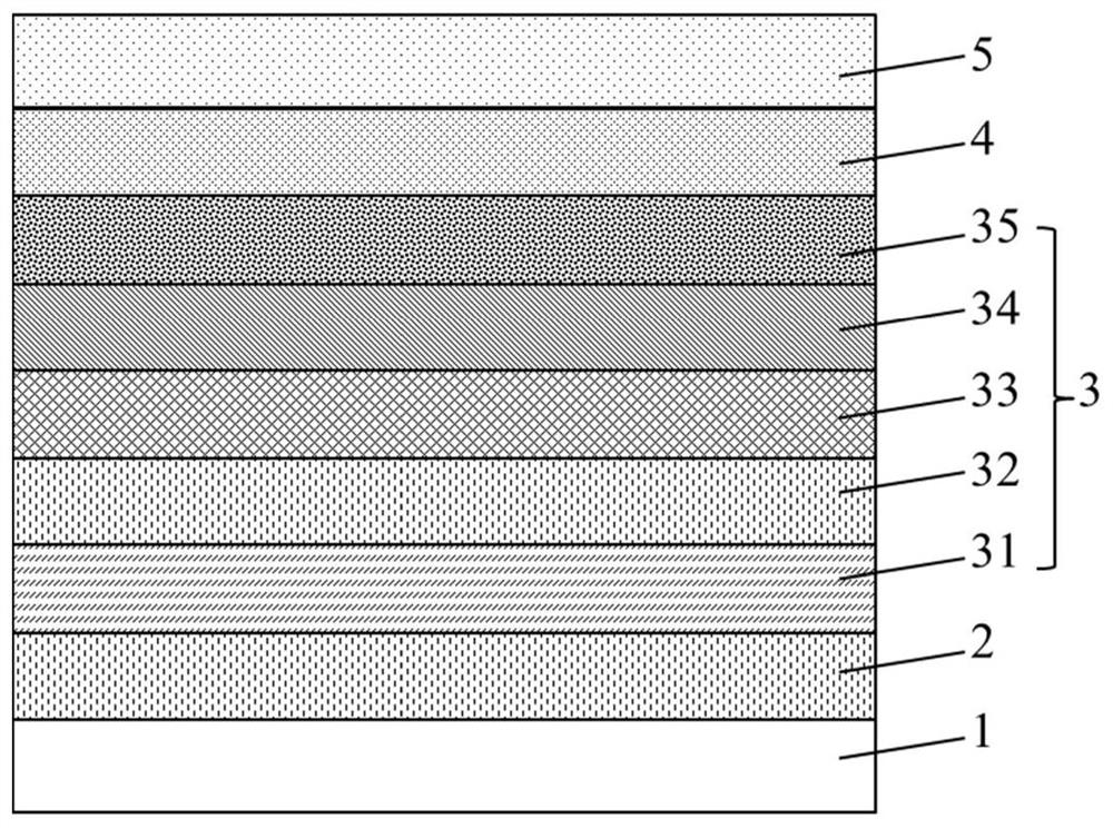
[0213] Anode 1 was prepared by the following process: the thickness of ITO was The ITO substrate was cut into a size of 40mm (length) × 40mm (width) × 0.7mm (thickness), and it was prepared into an experimental substrate with a cathode 5, an anode 1 and an insulating layer pattern by using a photolithography process, and using ultraviolet ozone and O 2 :N 2 The surface is treated with plasma to increase the work function of the anode 1, and the surface of the ITO substrate is cleaned with an organic solvent to remove impurities and oil stains on the surface of the ITO substrate. It should be noted that the ITO substrate can also be cut into other sizes according to actual needs, and the size of the ITO substrate in this application is not specifically limited here.
[0214] HAT-CN (see below for structural formula) was vacuum evaporated on the experimental substrate (anode 1) to form a thickness of ...
Embodiment 2~25
[0224] Except for using the compounds shown in Table 1 when forming the electron transport layer 35 (ETL), an organic electroluminescent device was fabricated by a method similar to that of Example 1, and the performance parameters of each device are shown in Table 1.
PUM
 Abstract
Description
Claims
Application Information
 - R&D
- Intellectual Property
- Life Sciences
- Materials
- Tech Scout
- Unparalleled Data Quality
- Higher Quality Content
- 60% Fewer Hallucinations
Browse by: Latest US Patents, China's latest patents, Technical Efficacy Thesaurus, Application Domain, Technology Topic, Popular Technical Reports.
© 2025 PatSnap. All rights reserved.Legal|Privacy policy|Modern Slavery Act Transparency Statement|Sitemap|About US| Contact US: help@patsnap.com


