Semiconductor device and manufacturing method thereof

A manufacturing method and semiconductor technology, applied in the fields of semiconductor/solid-state device manufacturing, electrical components, circuits, etc., can solve problems such as circuit short circuit, semiconductor device yield reduction, barrier dielectric layer deposition, etc., to achieve the effect of improving yield

Active Publication Date: 2022-05-31
WUHAN XINXIN SEMICON MFG CO LTD
View PDF7 Cites 0 Cited by
  • Summary
  • Abstract
  • Description
  • Claims
  • Application Information

AI Technical Summary

Problems solved by technology

[0004] After the self-aligned silicide is formed, a dielectric layer is filled in the trench, and the dielectric layer is filled by, for example, a HDP (high density plasma) deposition process. The particles on the surface of the sidewall of the trench and the oxide layer surrounding the particles are deposited in the HDP dielectric layer process. It will block the deposition of the dielectric layer and form voids in the trenches. The voids will lead to the subsequent interconnection between adjacent contact holes that should be insulated by the dielectric layer, forming a short circuit in the circuit, resulting in a reduction in the yield of semiconductor devices.

Method used


Image

  • Semiconductor device and manufacturing method thereof
  • Semiconductor device and manufacturing method thereof
  • Semiconductor device and manufacturing method thereof

Examples


Embodiment Construction

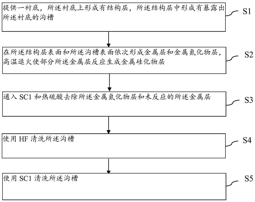
[0027] Embodiments of the present invention provide a semiconductor device and a manufacturing method thereof. Below in conjunction with the accompanying drawings and specific embodiments

[0029] providing a substrate on which a structural layer is formed, in which a structure layer exposing the substrate is formed

[0033] The trenches are cleaned using SC1.

[0034] The steps of the manufacturing method of the semiconductor device of the present embodiment are described below with reference to FIGS. 3 to 7 .

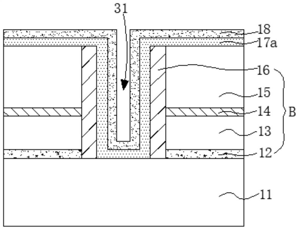
[0035] As shown in FIG. 3 and FIG. 4, a substrate 11 is provided on which a structural layer B is formed, and the structural layer B is

[0037] The substrate 11 can provide an operating platform for the subsequent process, which can be any use known to those skilled in the art.

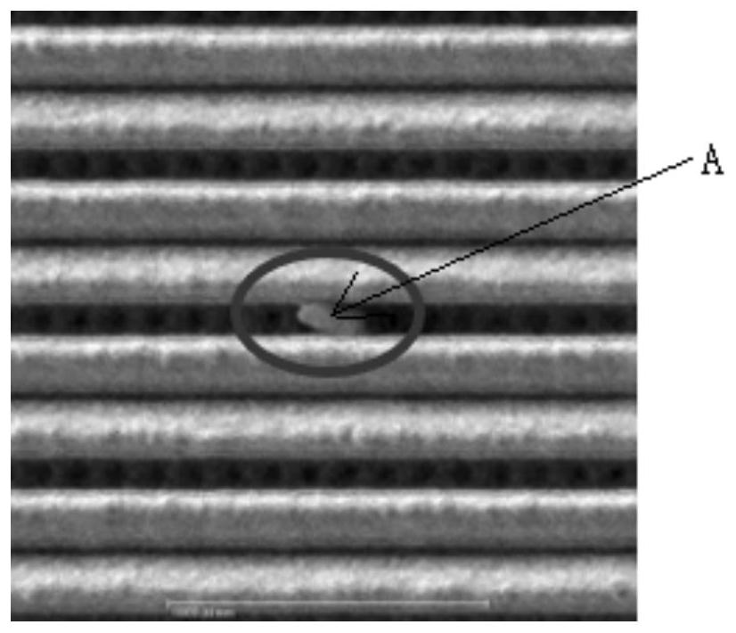
[0038] As shown in FIG. 3 to FIG. 5, the metal nitride layer 18 and the unreacted gold are removed by feeding SC1 and hot sulfuric acid.

[0039] As shown in FIG. 5 and FIG. 6, the surface of th...


PUM


Abstract

The present invention provides a semiconductor device and a manufacturing method thereof, comprising: providing a substrate, a structural layer is formed on the substrate, and a groove exposing the substrate is formed in the structural layer; A metal layer and a metal nitride layer are sequentially formed on the surface of the structural layer and the surface of the groove, and high-temperature annealing causes the metal layer to react to form a metal silicide layer; SC1 and hot sulfuric acid are introduced to remove the metal nitride layer and unreacted The metal layer; particles are formed on the sidewall of the groove, and an oxide layer is formed on the surface of the particle; the groove is cleaned with HF to remove the particles and the oxide layer; the SC1 is used to clean the The trench is used to completely remove the particles, and eliminate the void defect caused by the oxide layer enveloping the particles and adhering to the sidewall of the trench, thereby improving the yield of the semiconductor device.

Description

Semiconductor device and method of making the same technical field [0001] The present invention belongs to the technical field of integrated circuit manufacturing, and in particular relates to a semiconductor device and a manufacturing method thereof. Background technique In the integrated circuit manufacturing industry, salicide is widely used in the connection between source, drain, gate and metal [0002] Contact, salicide plays a very important role in large-scale and very large-scale CMOS logic integrated circuit technology. [0003] As shown in FIG. 1, trenches are formed between adjacent salicide structures, and conventional salicide structures are formed It is to deposit a layer of cobalt and titanium nitride first, and then react crystalline silicon and cobalt to form self-aligned silicide through high temperature reaction. Immediately after Then, hydrogen peroxide and sulfuric acid were introduced to remove titanium nitride and unreacted cobalt. However, when...

Claims


Application Information

Patent Timeline
Patent Type & Authority Patents(China)
IPC IPC(8): H01L21/02H01L21/285
CPCH01L21/02068H01L21/02071H01L21/28518
Inventor 黄胜男曹开玮李赟
Owner WUHAN XINXIN SEMICON MFG CO LTD
Why Eureka
Try Eureka