Preparation method of high-quality wafer-level graphene single crystal
A graphene and wafer-level technology, which is applied in the field of high-quality wafer-level graphene single crystal preparation, can solve the problems of time-consuming and consumable materials, complex process, harsh conditions, etc., and achieve short time-consuming, simple processing method and repeatability high effect
- Summary
- Abstract
- Description
- Claims
- Application Information
AI Technical Summary
Problems solved by technology
Method used
Image
Examples
Embodiment 1
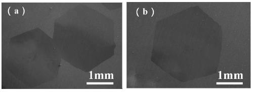
[0051] The difference between this Example 1 and Comparative Example 1 is that the electrochemically polished copper foil is subjected to plasma treatment, the plasma equipment is used, the air valve is opened, the power is adjusted to 100W, the pressure is stabilized between 400-500Pa, and the treatment time for 30 minutes. Other implementation methods are the same as Comparative Example 1. The resulting graphene single crystal SEM morphology is as follows figure 1 As shown in (b), it can be seen from the figure that the nucleation density of the graphene single crystal is effectively reduced, and there are only two graphene single crystals in the area in the figure. Experimental comparison shows that the number of graphene single crystal nucleation drops sharply after copper foil is treated by plasma. This method proves that plasma treatment can effectively control the nucleation density of graphene single crystal.
Embodiment 2
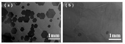
[0053] The copper foil is electrochemically polished, the electrolyte solution is pure phosphoric acid, the constant voltage is 3V, and the polishing time is 30 minutes. Then wash with deionized water and ethanol, and blow dry with nitrogen. The polished and cleaned copper foil is treated with plasma, the plasma equipment is used, the air valve is opened, the power is adjusted to 100W, the pressure is stabilized between 400-500Pa, and the treatment time is 30 minutes. Then put it into a chemical vapor deposition reaction furnace, feed 500 sccm argon gas, heat up to 1000°C, then feed 10 sccm hydrogen gas, anneal at constant temperature for 30 minutes, and introduce 10 sccm methane to react for 60 minutes. Turn off methane after reaction finishes, cool down to room temperature rapidly (cooling time is 20 minutes). The photo of the obtained graphene single crystal is shown in the figure figure 2 As shown in (a), and its graphene single crystal domain area is 1-2mm, the monolay...
Embodiment 3
[0055] The difference between the present embodiment 3 and the embodiment 2 is that the graphene single crystal is grown by temperature programming, and after the constant temperature annealing treatment, the graphene single crystal growth temperature is raised from 1000°C to 1080°C (the heating rate is about 1.3°C / min ) process imports carbon source, and the continuation reaction time is 60 minutes. Other implementation methods are the same as in Example 2. The photo of the obtained graphene single crystal is shown in the figure figure 2 As shown in (b), and its graphene single crystal domain area is about 5mm, the monolayer graphene coverage rate is 96%, and the mobility is 12000cm -2 v -1 the s -1 . Depend on figure 2 It can be seen that the temperature-programmed growth method can effectively accelerate the growth rate of graphene single crystal. Combined with Ranman ( image 3 ) and TEM ( Figure 4 ) shows that the prepared graphene single crystal has good cryst...
PUM
| Property | Measurement | Unit |
|---|---|---|
| thickness | aaaaa | aaaaa |
Abstract
Description
Claims
Application Information
 - R&D
- Intellectual Property
- Life Sciences
- Materials
- Tech Scout
- Unparalleled Data Quality
- Higher Quality Content
- 60% Fewer Hallucinations
Browse by: Latest US Patents, China's latest patents, Technical Efficacy Thesaurus, Application Domain, Technology Topic, Popular Technical Reports.
© 2025 PatSnap. All rights reserved.Legal|Privacy policy|Modern Slavery Act Transparency Statement|Sitemap|About US| Contact US: help@patsnap.com


