
Nano niobium aluminum yttrium nitride/amorphous silicon nitride dual-phase ultra-hard coating and a deposition method thereof

A technology of niobium aluminum yttrium nitride and crystalline silicon nitride, which is applied in coating, metal material coating process, ion implantation plating, etc., can solve the problem of weakening of dual-phase interface, low stability of Nb-Si-N solid solution, Weaken problems such as valence bond strength to achieve good heat resistance

Active Publication Date: 2019-11-12
JIANGXI SCI & TECH NORMAL UNIV
View PDF3 Cites 7 Cited by
  • Summary
  • Abstract
  • Description
  • Claims
  • Application Information

AI Technical Summary

Problems solved by technology

The second important reason is that even if a dual-phase composite structure can be formed, the existence of certain impurities in the coating will weaken the dual-phase interface. For example, there is a certain amount of O impurities in the coating, and the highly electronegative O and Si The combination of Si-O bonds will weaken the valence bond strength of the neighbors, and the hardness of the coating can only reach 35GPa or even lower; in addition, the Si-O bond will limit the decomposition of TM-Si-N solid solution and the nc-TMN / a-Si 3 N 4 Formation
The Nb-Si-N solid solution has low stability and is more prone to phase separation at lower temperatures to form nanocrystalline NbN implanted in amorphous Si 3 N 4 composite structure

Method used


Image

  • Nano niobium aluminum yttrium nitride/amorphous silicon nitride dual-phase ultra-hard coating and a deposition method thereof

Examples


Embodiment 1

[0021] Carbide PCB micro-drill, with a shank diameter of 3.175mm and a blade diameter of 0.2mm, is loaded into the coating furnace after degreasing, organic solvent cleaning, deionized water rinsing, and drying. Vacuum to 1.0×10 -3 Below Pa, the temperature is kept at 200±5℃. The first step is to perform gas plasma cleaning on the workpiece substrate: Ar and H are introduced into the gas ion source 2 , the partial pressure is 0.2Pa and 0.1Pa respectively, the ion source current is 5A, the workpiece is applied with pulse negative bias voltage, the frequency is 80KHz, the peak value is 100V, the duty cycle is 90%, and the workpiece is plasma cleaned for 30min. The second step is to perform arc plasma cleaning on the workpiece: turn off the gas ion source, adjust the pulse negative bias to a frequency of 80KHz, a peak value of 700V, a duty cycle of 30%, Ar and H 2 The partial pressure was adjusted to 0.1Pa and 0.05Pa, the arc ion plating Nb target was turned on, the arc source ...

Embodiment 2

[0023] Carbide PCB micro-drill, with a shank diameter of 3.175mm and a blade diameter of 0.35mm, is loaded into the coating furnace after degreasing, organic solvent cleaning, deionized water rinsing, and drying. Vacuum to 1.0×10 -3 Below Pa, the temperature is kept at 200±5℃. The first step is to perform gas plasma cleaning on the workpiece substrate: Ar and H are introduced into the gas ion source 2 , the partial pressure is 0.2Pa and 0.1Pa respectively, the ion source current is 5A, the workpiece is applied with pulse negative bias voltage, the frequency is 80KHz, the peak value is 150V, the duty cycle is 90%, and the workpiece is plasma cleaned for 30min. The second step is to perform arc plasma cleaning on the workpiece: turn off the gas ion source, adjust the pulse negative bias to a frequency of 80KHz, a peak value of 800V, a duty cycle of 30%, Ar and H 2 The partial pressure was adjusted to 0.1Pa and 0.05Pa, the arc ion plating Nb target was turned on, the arc source...

Embodiment 3

[0025] Carbide PCB milling cutter, with a shank diameter of 3.175mm and a blade diameter of 1.2mm, is loaded into the coating furnace after degreasing, organic solvent cleaning, deionized water rinsing, and drying. Vacuum to 1.5×10 -3 Below Pa, the temperature is kept at 250±5℃. The first step is to perform gas plasma cleaning on the workpiece substrate: Ar and H are introduced into the gas ion source 2 , the partial pressures are 0.2Pa and 0.1Pa respectively, the ion source current is 8A, the workpiece is applied with pulse negative bias, the frequency is 80KHz, the peak value is 200V, and the duty cycle is 90%, and the workpiece is plasma cleaned for 30min. The second step is to perform arc plasma cleaning on the workpiece: turn off the gas ion source, adjust the pulse negative bias to a frequency of 80KHz, a peak value of 1000V, a duty cycle of 30%, Ar and H 2 The partial pressure was adjusted to 0.1Pa and 0.05Pa, the arc ion plating Nb target was turned on, the arc sourc...


PUM

PropertyMeasurementUnit
thicknessaaaaaaaaaa
thicknessaaaaaaaaaa
thicknessaaaaaaaaaa

Abstract

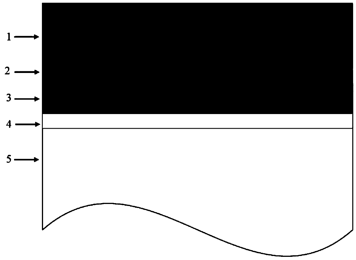
The invention relates to a nano niobium aluminum yttrium nitride / amorphous silicon nitride dual-phase ultra-hard coating and a deposition method thereof. The ultra-hard coating is of a four-layer structure, wherein the innermost layer is a pure niobium bonding layer, and thickness of the innermost layer is 0.05-0.5 micron; the secondary inner layer is a niobium nitride transition layer, and the thickness of the secondary inner layer is 0.05-1 micron; the secondary outer layer is a gradient layer, component of the niobium nitride is gradually reduced from inside to outside, and components of the niobium aluminum yttrium nitride / the silicon nitride are gradually increased, the thickness of the secondary outer layer is about 0.1-1.0 micron, and concentration on a stress interface can be prevented; and the outermost layer is composite wear-resistant layer of the niobium aluminum yttrium nitride / the silicon nitride, the thickness of the composite wear-resistant layer is 1-10 microns. The total thickness of the coating is 1.2-12.5 microns. Binding force of the coating and a hard alloy matrix reaches 70-105 N, hardness of the coating is 40-60 GPa, friction coefficient of the coating is 0.20-0.55, antioxidant temperature of the coating is 750 DEG C or higher, and service life of a coated micro drill or milling cutter is prolonged by 4-8 times compared with that of an uncoated micro drill or milling cutter.

Description

technical field [0001] The invention relates to a nano-niobium-aluminum-yttrium nitride / amorphous silicon nitride dual-phase superhard coating for hard alloy cutting tools and a deposition method thereof, belonging to the fields of machining and new materials. Background technique [0002] With the huge development of the printed circuit board (PCB) industry, the consumption of milling cutters and micro-drills for PCB processing in mainland China has reached billions of pieces every year. In recent years, the increase in the number of layers of the circuit board, the improvement of the cutting rate, and the large-scale application of halogen-free and other difficult-to-drill materials have put forward higher requirements for the cutting performance of milling cutters and micro-drills, prompting people to explore suitable PCB milling cutters and micro-drills. surface strengthening technology. For fine-grained carbide PCB milling cutters and micro-drills whose Vickers hardnes...

Claims


Application Information

Patent Timeline
Patent Type & Authority Applications(China)
IPC IPC(8): C23C14/02C23C14/16C23C14/06C23C14/32
CPCC23C14/0021C23C14/025C23C14/0641C23C14/16C23C14/325
Inventor 李明升张琳英易家骏陈土春吴志诚
Owner JIANGXI SCI & TECH NORMAL UNIV
Learn More