High-gain solar blind ultraviolet light detector based on (GaY)2O3 amorphous film and preparation method of high-gain solar blind ultraviolet light detector
An amorphous thin-film, high-gain technology, applied in photovoltaic power generation, semiconductor devices, final product manufacturing, etc., can solve the problems of crystal quality degradation, device performance and stability, etc., and achieve improved response, reduced dark current, relaxation The effect of delay time reduction
- Summary
- Abstract
- Description
- Claims
- Application Information
AI Technical Summary
Problems solved by technology
Method used
Image
Examples
Embodiment 1
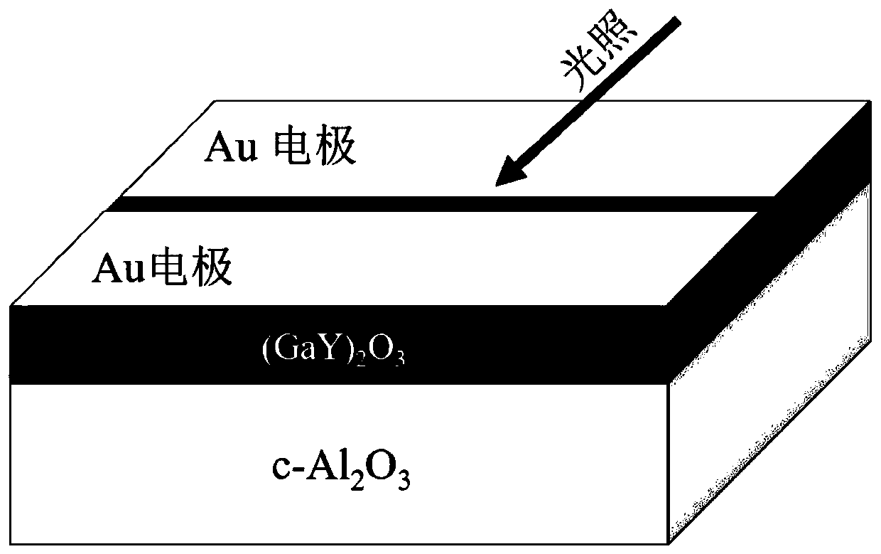
[0046] Such as figure 1 As shown, a (GaY) based 2 o 3 A high-gain solar-blind ultraviolet light detector of an amorphous film, the detector includes a c-plane sapphire substrate, an active layer, and a pair of parallel metal Au electrodes from bottom to top, wherein: the active layer is amorphous ( GaY) 2 o 3 film. The thickness of the substrate is 0.43 mm, the thickness of the active layer is 150 nm, the thickness of the Au electrodes is 50 nm, and the distance between the parallel electrodes is 10 μm.
[0047] The above-mentioned (GaY) based 2 o 3 The high-gain solar-blind ultraviolet light detector of the amorphous film is prepared by the following method, including the following steps:
[0048] Step 1: Preparation of (GaY) by solid phase sintering method 2 o 3 Ternary ceramic target
[0049] 1.1 molar ratio Ga 2 o 3 : Y 2 o 3 =70:30, weigh 6.595g Ga 2 o 3 powder and 3.401gY 2 o 3 Powder, after mixing, add 15g of deionized water, then place in the ball mil...
Embodiment 2
[0059] A (GaY) based 2 o 3 A sun-blind ultraviolet light detector of a ternary alloy, the detector includes a c-plane sapphire substrate, an active layer, and a pair of parallel metal Au electrodes from bottom to top, wherein: the active layer is (GaY) 2 o 3 thin film, the thickness of the substrate is 0.43mm, the thickness of the active layer is 150nm, the thickness of the electrodes is 55nm, and the distance between the parallel electrodes is 10 μm.
[0060] The above-mentioned (GaY) based 2 o 3 The thin-film sun-blind ultraviolet light detector is prepared by the following method, including the following steps:
[0061] Step 1: Preparation of (GaY) by solid phase sintering method 2 o 3 Ternary ceramic target
[0062] 1.1 molar ratio Ga 2 o 3 : Y 2 o 3 =95:5, weigh 9.403g Ga 2 o 3 powder and 0.596g Y 2 o 3 Powder, after mixing, add 15g of deionized water, then place in the ball mill jar (the ball milling medium is zirconia ceramic balls) in the planetary ball ...
Embodiment 3
[0071] A (GaY) based 2 o 3 A sun-blind ultraviolet light detector of a ternary alloy, the detector includes a c-plane sapphire substrate, an active layer, and a pair of parallel metal Al electrodes from bottom to top, wherein: the active layer is (GaY) 2 o 3 For the ternary alloy thin film, the thickness of the substrate is 0.43mm, the thickness of the active layer is 300nm, the thickness of the electrodes is 30nm, and the distance between the parallel electrodes is 50μm.
[0072] The above-mentioned (GaY) based 2 o 3 The thin-film sun-blind ultraviolet light detector is prepared by the following method, including the following steps:
[0073] Step 1: Prepare (GaY) by the same solid phase sintering method as in Example 1 2 o 3 Ternary ceramic target.
[0074] Step 2: Utilize (GaY) 2 o 3 Preparation of solar-blind ultraviolet light detectors with ternary ceramic targets
[0075] 2.1 (GaY) prepared in step 1 2 o 3 Ternary ceramics are used as laser ablation targets, ...
PUM
 Abstract
Description
Claims
Application Information
 - R&D
- Intellectual Property
- Life Sciences
- Materials
- Tech Scout
- Unparalleled Data Quality
- Higher Quality Content
- 60% Fewer Hallucinations
Browse by: Latest US Patents, China's latest patents, Technical Efficacy Thesaurus, Application Domain, Technology Topic, Popular Technical Reports.
© 2025 PatSnap. All rights reserved.Legal|Privacy policy|Modern Slavery Act Transparency Statement|Sitemap|About US| Contact US: help@patsnap.com


