Transition metal chalcogenide film and preparation method and application thereof
A technology of transition metal chalcogenides and transition metals, which is applied in the field of transition metal chalcogenide thin films and their preparation, which can solve the unpredictable application of elements with different properties, the inability to obtain large-size two-dimensional materials, and the inability to obtain two-dimensional nano-films, etc. problems, to achieve continuous and controllable growth, easy control, and excellent performance
- Summary
- Abstract
- Description
- Claims
- Application Information
AI Technical Summary
Problems solved by technology
Method used
Image
Examples
preparation example Construction
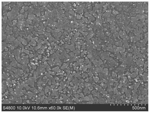
[0060] The preparation method comprises: separately heating a platinum group metal source and a chalcogen element source in a protective gas atmosphere to generate a chemical vapor deposition reaction, and grow a transition metal chalcogen compound thin film on a substrate.
[0061] In addition, in the embodiment of the present invention, a tubular heating furnace is used to carry out the chemical vapor deposition reaction, wherein the length of the quartz tube is 1.2 m, and the diameter is 1 inch. There are vacuum valves at both ends of the quartz tube, and the quartz tube is longer than that of the tubular heating furnace. The silicon chip used in the embodiment is a commercially available silicon chip, which is a high-phosphorus silicon chip produced by Hefei Kejing Technology Co., Ltd., its resistance value is 0.02~0.6Ω, and its size is 0.5mm×4 inches.
Embodiment 1
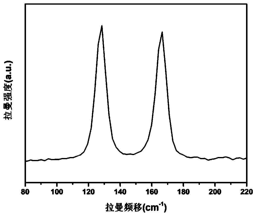
[0064] This embodiment provides a method for preparing a transition metal chalcogenide film, wherein the transition metal is iridium, and the chalcogen element is tellurium.
[0065] Its preparation method comprises the following steps:
[0066] (1) After oxidizing the surface of commercially purchased silicon wafers, cut them into small pieces, peel the boron nitride single crystal onto the cut silicon wafers by mechanical peeling method, and anneal at 500 ° C for 1 hour to obtain boron nitride substrates;
[0067] (2) 0.0209g iridium acetylacetonate, 5.0107g tellurium powder and 6 boron nitride substrates are placed in the quartz tube according to the flow direction of the gas, wherein the iridium acetylacetonate is placed in the quartz tube outside the heating furnace body, and used The heating sheet wraps this part of the quartz tube, the tellurium powder is placed in the quartz tube at a distance of 18cm from the center, and the base is placed in the middle of the quartz ...
Embodiment 2
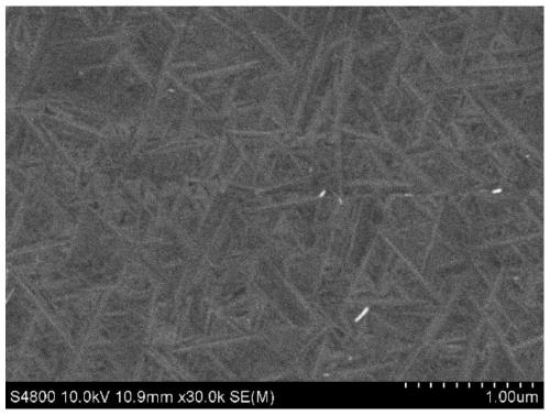
[0072] This embodiment provides a method for preparing a transition metal chalcogenide film, wherein the transition metal is iridium, and the chalcogen element is tellurium.
[0073] Its preparation method comprises the following steps:
[0074] (1) After oxidizing the surface of commercially available silicon wafers, cut them into small pieces of 6×8mm, use the mechanical stripping method to peel boron nitride single crystals onto the cut silicon wafers, and anneal at 550°C for 0.8h to obtain nitrided silicon wafers. Boron substrate;
[0075] (2) 0.0185g iridium acetylacetonate, 2.2571g tellurium powder and 6 boron nitride substrates are placed in the quartz tube according to the flow direction of the gas, wherein iridium acetylacetonate is placed in the quartz tube outside the heating furnace body, and used The heating sheet wraps this part of the quartz tube, the tellurium powder is placed in the quartz tube at a distance of 17cm from the center, and the base is placed in ...
PUM
| Property | Measurement | Unit |
|---|---|---|
| thickness | aaaaa | aaaaa |
| electrical resistance | aaaaa | aaaaa |
| size | aaaaa | aaaaa |
Abstract
Description
Claims
Application Information
 - Generate Ideas
- Intellectual Property
- Life Sciences
- Materials
- Tech Scout
- Unparalleled Data Quality
- Higher Quality Content
- 60% Fewer Hallucinations
Browse by: Latest US Patents, China's latest patents, Technical Efficacy Thesaurus, Application Domain, Technology Topic, Popular Technical Reports.
© 2025 PatSnap. All rights reserved.Legal|Privacy policy|Modern Slavery Act Transparency Statement|Sitemap|About US| Contact US: help@patsnap.com


