Single-transistor active pixel sensor based on silicon-on-insulator layer and its preparation method
A technology of pixel sensor and silicon on insulating layer, which is applied in the field of new single-transistor active pixel sensor and its preparation, can solve the problems of increasing the complexity of the sensing unit, reducing the sensitivity of the sensor, and losing the sensing area, etc., and achieves the purpose of increasing the effective sensing Sensitive area, reduced complexity, and high sensitivity effects
- Summary
- Abstract
- Description
- Claims
- Application Information
AI Technical Summary
Problems solved by technology
Method used
Image


Examples
preparation example Construction
[0050] Such as Figure 2a-Figure 2f In conjunction with shown, the invention provides a kind of preparation method of semiconductor photoelectric sensor, concrete steps are as follows:
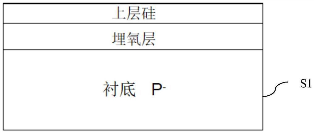
[0051] S1. Prepare the initial silicon-on-insulator layer, the silicon-on-insulator layer includes a substrate 1, a buried oxide layer 2, and a channel layer 3;
[0052] S2, photolithography, etching, and polishing after depositing an oxide layer to form isolation 4 (shallow trench isolation area);
[0053] S3, deposit positive gate oxide layer 5 and positive gate material, perform photolithography and etch to form the pattern of positive gate 6;
[0054] S4, after forming gate spacer and source and drain epitaxy, photolithography and implanting N-type doped ions to form heavily doped source region 7 and heavily doped drain region 8 (for example, N-type doping) ;
[0055] S5, photolithography and implanting P-type doped ions to form a back gate heavily doped region, and high-temperature ann...
Embodiment 1
[0059] In the step S1, in the initial silicon-on-insulator wafer, the doping of the substrate 1 is generally weakly p-type doped silicon with a doping concentration of 10 15 cm -2 to 10 17 cm -2 between. Depending on the sensing optical wavelength, the substrate 1 can also be made of silicon germanium, gallium nitride, or indium gallium arsenic; the buried oxide layer 2 is generally silicon dioxide, with a thickness between 10nm and 1000nm; the upper channel Layer 3 is generally made of materials such as silicon, silicon germanium, gallium nitride or indium gallium arsenic, with a thickness between 2nm and 100nm.
[0060] The step S2 specifically includes: after photolithography and opening the window of the isolation trench, etching using the photoresist as a mask to form the pattern of the isolation trench.
[0061] Wherein, etching may be performed by dry etching or wet etching. The dry etching generally uses fluorine-based or halogen gas, such as SF 6 、CHF 3 , HBr o...
Embodiment 2
[0068] The second embodiment is similar to the first embodiment, except that the channel of the first embodiment is based on a P-type MOSFET instead of an N-type. The source region 7, the drain region 8 and the back gate contact region 9 are all heavily P-type doped. Therefore, the process flow of this embodiment is similar to the first embodiment, only step S4 and step S5 need to be changed to simultaneously open the source region 7, drain region 8 and back gate contact region 9 during photolithography, and then implant P-type ions , such as boron or BF 2 , and the injection dose and energy of each window are the same as those in Embodiment 1, and the others are similar to Embodiment 1, and will not be repeated here.
[0069] From the above, the present invention is based on deep depletion and in-situ charge-sensing single-transistor active pixel sensor built on a fully depleted silicon-on-insulator substrate, and the thickness of the silicon layer of the channel can be belo...
PUM
| Property | Measurement | Unit |
|---|---|---|
| thickness | aaaaa | aaaaa |
| thickness | aaaaa | aaaaa |
| thickness | aaaaa | aaaaa |
Abstract
Description
Claims
Application Information
 - R&D
- Intellectual Property
- Life Sciences
- Materials
- Tech Scout
- Unparalleled Data Quality
- Higher Quality Content
- 60% Fewer Hallucinations
Browse by: Latest US Patents, China's latest patents, Technical Efficacy Thesaurus, Application Domain, Technology Topic, Popular Technical Reports.
© 2025 PatSnap. All rights reserved.Legal|Privacy policy|Modern Slavery Act Transparency Statement|Sitemap|About US| Contact US: help@patsnap.com