Back side processing method of power semiconductor device
A technology of power semiconductors and processing technology, which is applied in the direction of semiconductor devices, semiconductor/solid-state device manufacturing, electrical components, etc., can solve problems such as unresolved problems, and achieve increased activation rate, low conduction voltage drop, and high current-carrying area of the collector area The effect of subconcentration
- Summary
- Abstract
- Description
- Claims
- Application Information
AI Technical Summary
Problems solved by technology
Method used
Image
Examples
Embodiment 1
[0036] A back processing technology of a power semiconductor device comprises the steps of:
[0037] After forming a collector region and a buffer layer on the back surface of the semiconductor substrate of the first conductivity type,
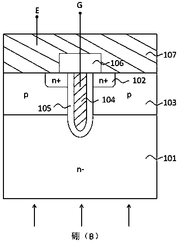
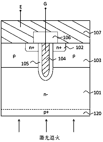
[0038] The first step is to carry out the manufacturing process of the collector region of the second conductivity type, including the implantation process and the formation process. The implantation process is: the first type of ion implantation is performed from the back of the semiconductor substrate of the first conductivity type; the formation process is: performing laser annealing on the semiconductor substrate, thereby forming a first region of the second conductivity type having a higher carrier concentration than the semiconductor substrate of the first conductivity type on the back surface of the semiconductor substrate;
[0039] The second step is to perform a buffer layer manufacturing process, including an implantation process and...
Embodiment 2
[0042] A back processing technology of a power semiconductor device, comprising the steps of:
[0043] After forming a collector region and a buffer layer on the back surface of the semiconductor substrate of the first conductivity type,
[0044] The first step is to carry out the manufacturing process of the collector region of the second conductivity type, including the implantation process and the formation process. The implantation process is: the first type of ion implantation is performed from the back of the semiconductor substrate of the first conductivity type; the formation process is: performing laser annealing on the semiconductor substrate, thereby forming a first region of the second conductivity type having a higher carrier concentration than the semiconductor substrate of the first conductivity type on the back surface of the semiconductor substrate;
[0045] The second step is to perform a buffer layer manufacturing process, including an implantation process a...
Embodiment 3
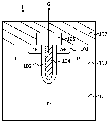
[0051] Figure 1 to Figure 6 A first embodiment of the present invention is shown. Such as figure 1 As shown, the semiconductor device IGBT has completed all the front-side processes of the chip, including the trench gate MOS structure, and the back-side thinning process. After thinning, the chip thickness is 120 μm. The first conductivity type is n-type, the second conductivity type is p-type, the semiconductor silicon substrate is the n-type drift region 101 of the device, and the carrier concentration of the drift region 101 is 7E13cm -3 The formed front structure includes an n-type emitter region 102, a p-type base region 103, a trench gate 104, a gate oxide 105, an insulating layer 106 and a front metal electrode 107, and the front power MOS structure is manufactured using the front structure of a semiconductor device. General methods and conventional means are not described in detail here. The backside process starts with thinning the backside of the semiconductor sub...
PUM
 Abstract
Description
Claims
Application Information
 - R&D
- Intellectual Property
- Life Sciences
- Materials
- Tech Scout
- Unparalleled Data Quality
- Higher Quality Content
- 60% Fewer Hallucinations
Browse by: Latest US Patents, China's latest patents, Technical Efficacy Thesaurus, Application Domain, Technology Topic, Popular Technical Reports.
© 2025 PatSnap. All rights reserved.Legal|Privacy policy|Modern Slavery Act Transparency Statement|Sitemap|About US| Contact US: help@patsnap.com


