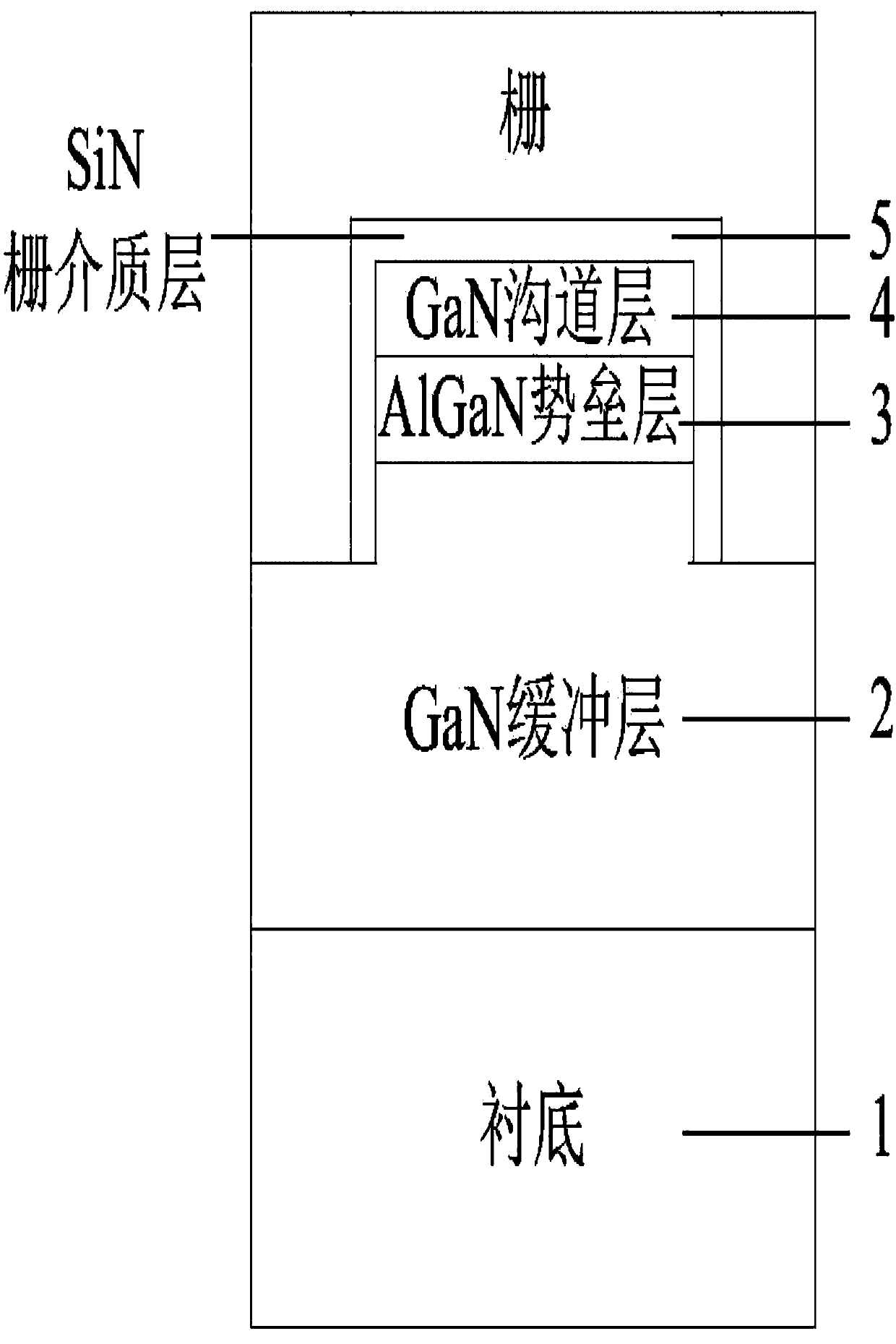
T-gate N-plane GaN/AlGaN fin high electron mobility transistor
A high electron mobility, transistor technology, applied in circuits, electrical components, semiconductor devices, etc., can solve the problems of weak short channel effect suppression ability, poor two-dimensional electron gas confinement, high ohmic contact resistance, etc., to achieve Suppression of short channel effect, improvement of microwave performance, and small ohmic contact resistance
- Summary
- Abstract
- Description
- Claims
- Application Information
AI Technical Summary
Problems solved by technology
Method used
Image
Examples
Embodiment 1
[0028] Example 1: Fabricate a T-gate N-plane GaN / AlGaN fin-type high electron mobility transistor with a fin-type GaN / AlGaN heterojunction width of 2 μm, a T-type gate neck height of 50 nm, and a gate cap height of 100 nm.
[0029] Step 1: growing a buffer layer.
[0030] At a temperature of 680°C and a pressure of 5×10 -3 Under the process condition of Pa, the molecular beam epitaxy MBE equipment is used in Figure 4 (a) An N-face GaN buffer layer with a thickness of 1.5 μm is grown on the sapphire substrate shown in (a).
[0031] Step 2: growing a barrier layer.
[0032] At a temperature of 680°C and a pressure of 5×10 -3 Under the process conditions of Pa, a layer of AlGaN with a thickness of 20nm was first grown on the GaN layer by using molecular beam epitaxy MBE equipment, and the Al composition gradually changed from 5% to 30% from bottom to top; The composition is 30% AlGaN layer.
[0033] Step 3: growing a channel layer.
[0034] At a temperature of 680°C and a ...
Embodiment 2
[0047] Example 2: Fabricate a T-gate N-plane GaN / AlGaN fin-type high electron mobility transistor with a fin-type GaN / AlGaN heterojunction width of 3 μm, a T-type gate neck height of 70 nm, and a gate cap height of 200 nm.
[0048] Step 1: Growth buffer layer.
[0049] On the SiC substrate, a layer of N-face GaN buffer layer with a thickness of 2 μm is grown by molecular beam epitaxy MBE. The growth process conditions are:
[0050] The growth temperature is 680°C and the pressure is 5×10 -3 Pa.
[0051] Step 2: Growing a barrier layer.
[0052] A layer of AlGaN with a thickness of 20nm was grown on the GaN layer by MBE, and the Al composition gradually changed from 5% to 30% from bottom to top; another layer of AlGaN with a thickness of 8nm and an Al composition of 30% was grown layer, the process conditions for its growth are:
[0053] The growth temperature is 680°C and the pressure is 5×10 -3 Pa.
[0054] Step 3: growing a channel layer.
[0055] On the AlGaN layer, ...
Embodiment 3
[0067] Example 3: Fabricate a T-gate N-plane GaN / AlGaN fin-type high electron mobility transistor with a fin-type GaN / AlGaN heterojunction width of 2.5 μm, a T-type gate neck height of 90 nm, and a gate cap height of 250 nm.
[0068] Step A: growing a buffer layer on the substrate.
[0069] Using molecular beam epitaxy MBE equipment at a temperature of 680°C and a pressure of 5×10 -3 Under the process condition of Pa, an N-face GaN buffer layer with a thickness of 2.5 μm is grown on the SiC substrate.
[0070] Step B: growing a barrier layer on the buffer layer.
[0071] Using molecular beam epitaxy MBE equipment at a temperature of 680°C and a pressure of 5×10 -3 Under the process conditions of Pa, a layer of AlGaN with a thickness of 20nm is first grown on the GaN buffer layer, and the Al composition is gradually changed from 5% to 30% from bottom to top, and the thickness of another layer is 5nm, and the Al composition is 30%. AlGaN layer.
[0072] Step C: growing a cha...
PUM
 Abstract
Description
Claims
Application Information
 - R&D Engineer
- R&D Manager
- IP Professional
- Industry Leading Data Capabilities
- Powerful AI technology
- Patent DNA Extraction
Browse by: Latest US Patents, China's latest patents, Technical Efficacy Thesaurus, Application Domain, Technology Topic, Popular Technical Reports.
© 2024 PatSnap. All rights reserved.Legal|Privacy policy|Modern Slavery Act Transparency Statement|Sitemap|About US| Contact US: help@patsnap.com


