N-type crystalline silicon solar cell and preparation method thereof, and photovoltaic module
A technology of solar cells and crystalline silicon, applied in the field of solar cells, can solve the problem of high carrier recombination rate, achieve the effect of improving cost performance, increasing voltage and current, and reducing the cost of electricity
- Summary
- Abstract
- Description
- Claims
- Application Information
AI Technical Summary
Problems solved by technology
Method used
Image
Examples
preparation example Construction
[0087] A method for preparing an N-type crystalline silicon solar cell provided in an embodiment of the present invention includes the following steps:
[0088] Step S1, providing an N-type crystalline silicon substrate 1;
[0089] Step S2, forming an emitter 3 on the front surface of the N-type crystalline silicon substrate 1;
[0090] In step S3 , a gallium oxide layer 21 in direct contact with the emitter 3 is formed on the emitter 3 .
[0091] As mentioned above, in the N-type crystalline silicon solar cell prepared by the preparation method provided by the embodiment of the present invention, the negatively charged gallium oxide layer 21 is directly in contact with the P-type silicon surface (in an N-type crystalline silicon solar cell, the emission Extremely P-type silicon), on the one hand, chemical passivation and field passivation are carried out on the surface of P-type silicon, thereby reducing the recombination rate of minority carriers at the surface of P-type si...
Embodiment 1
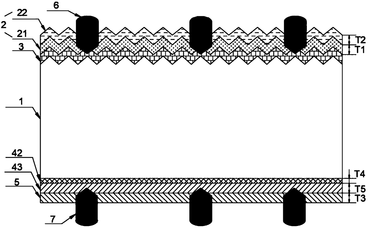
[0112] This embodiment provides a gallium oxide passivated N-type crystalline silicon double-sided solar cell, such as figure 2 As shown, the solar cell includes a front electrode 6, a front passivation layer 2, an emitter 3, and an N-type crystalline silicon substrate 1 arranged in sequence from the front (ie, the light-receiving surface of the solar cell) to the back (ie, the backlight surface of the solar cell). , N-type doped layer 41 , back passivation layer 5 and back electrode 7 .
[0113] Wherein, the N-type crystalline silicon substrate 1 is an N-type single crystal silicon wafer with a resistivity of 2.0Ω·cm and a size of 156.75mm×156.75mm. The emitter 3 is formed by boron diffusion in the furnace tube, and the sheet resistance value after doping is 80Ω / □.
[0114] The front passivation layer 2 includes a gallium oxide layer 21 in direct contact with the emitter 3 and a silicon nitride capping layer 22 disposed on the gallium oxide layer 21, wherein the thickness o...
Embodiment 2
[0130] This embodiment provides a gallium oxide passivated N-type crystalline silicon double-sided solar cell. The difference between the solar cell provided in this embodiment and the solar cell provided in Embodiment 1 is that the gallium oxide in the solar cell provided in this embodiment The thickness of the layer is 1 nm.
[0131] According to the test method and test conditions of Example 1, the performance of the solar cell provided in this example was tested, and the results were: open circuit voltage 0.661V, short circuit current 9.79A, and photoelectric conversion efficiency 20.92%.
PUM
 Abstract
Description
Claims
Application Information
 - R&D
- Intellectual Property
- Life Sciences
- Materials
- Tech Scout
- Unparalleled Data Quality
- Higher Quality Content
- 60% Fewer Hallucinations
Browse by: Latest US Patents, China's latest patents, Technical Efficacy Thesaurus, Application Domain, Technology Topic, Popular Technical Reports.
© 2025 PatSnap. All rights reserved.Legal|Privacy policy|Modern Slavery Act Transparency Statement|Sitemap|About US| Contact US: help@patsnap.com


