Group III/nitride epitaxial structure and its active device and its integrated method
A gallium nitride epitaxy and gallium nitride technology, which is used in semiconductor/solid-state device manufacturing, electrical components, semiconductor devices, etc., can solve the problems of difficult to control the etching depth and uneven thickness of the epitaxial layer of the epitaxial chip.
- Summary
- Abstract
- Description
- Claims
- Application Information
AI Technical Summary
Problems solved by technology
Method used
Image
Examples
Embodiment 2
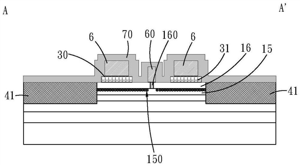
[0131] Embodiment two: as Figure 5A , 5B , for the fluorine ion implantation-enhanced aluminum gallium nitride / gallium nitride (AlGaN / GaN) high-speed electron mobility transistor of the present invention is connected in series with depletion type and does not have gate insulating dielectric layer gallium aluminum nitride / gallium nitride (AlGaN AlGaN / GaN) high-speed electron mobility transistors are the first structure diagram and the second structure diagram of the fluorine ion implanted mixed enhanced aluminum gallium nitride / gallium nitride (AlGaN / GaN) high-speed electron mobility transistor. Such as Figure 5A , 5B As shown, fluorine ions (F-) are implanted in the aluminum gallium nitride barrier layer (i-AlGaN barrier layer) 16 under the first gate electrode metal 60 to form an enhanced aluminum gallium nitride / gallium nitride (AlGaN / GaN) high-speed electron mobility transistor connected in series with a depletion-type aluminum gallium nitride / gallium nitride (AlGaN / G...
Embodiment 4
[0155] The manufacturing process of the fourth embodiment is the same as that of the previous embodiments in that after the fluorine ion implantation process is performed on the aluminum gallium nitride / gallium nitride (AlGaN / GaN) epitaxial structure designed in the present invention, the fourth embodiment is formed in the left region L1. A source ohmic contact electrode 30 and a first drain ohmic contact electrode 31 synchronously form a cathode ohmic contact electrode (cathode electrode metal) 34 of a Schottky barrier diode (SBD) in the right region R1. An anode field plate insulating dielectric layer 92 is then formed on the right region R1 , and the first gate insulating dielectric layer 50 is also formed in the left region L1 at this time.
[0156] Next, as previously mentioned, form the first gate electrode metal 60 and each connection metal, for example: the first gate of the fluorine ion implanted hybrid aluminum gallium nitride / gallium nitride (AlGaN / GaN) Schottky barr...
PUM
| Property | Measurement | Unit |
|---|---|---|
| thickness | aaaaa | aaaaa |
Abstract
Description
Claims
Application Information
 - R&D Engineer
- R&D Manager
- IP Professional
- Industry Leading Data Capabilities
- Powerful AI technology
- Patent DNA Extraction
Browse by: Latest US Patents, China's latest patents, Technical Efficacy Thesaurus, Application Domain, Technology Topic, Popular Technical Reports.
© 2024 PatSnap. All rights reserved.Legal|Privacy policy|Modern Slavery Act Transparency Statement|Sitemap|About US| Contact US: help@patsnap.com


