High performance memristive device based on metal oxide oxygen concentration gradient and its fabrication
A technology of memristive devices and oxides, applied in electrical components and other directions, can solve problems such as increased power consumption, discrete distribution, and increased circuit area, and achieve the effects of preventing electrical crosstalk, long retention time, and high computing speed.
- Summary
- Abstract
- Description
- Claims
- Application Information
AI Technical Summary
Problems solved by technology
Method used
Image
Examples
preparation example Construction
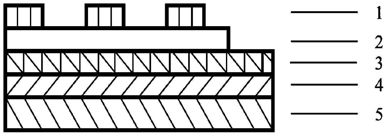
[0045] Generally speaking, the preparation method can be specifically prepared by sputtering to prepare the lower electrode, on the lower electrode, the functional layer is prepared by photolithography, sputtering, and peeling, and on the functional layer, the upper electrode is prepared by photolithography, sputtering, and peeling. , so as to form a memristor device with a three-layer structure; among them, when preparing the functional layer by sputtering, it is necessary to adjust Ar and O during the sputtering process 2 The proportion of oxygen concentration gradient functional layer. For example, the following steps may be included:
[0046] (1) preparing the lower electrode;
[0047] By the method of magnetron sputtering, SiO is grown on one side polished 2 A layer of metal lower electrode is grown on the monocrystalline silicon substrate, and the obtained lower electrode film can cover the entire substrate surface, and the total thickness can be 50nm-200nm;
[0048] ...
Embodiment 1
[0067] Taking a tantalum-based memristive device as an example, the corresponding preparation method may include the following steps:
[0068] (1) preparing the lower electrode;
[0069] In the experiment, Ta was selected as the lower electrode, and SiO was grown on one side by magnetron sputtering. 2 A lower electrode is grown on a single crystal silicon substrate.
[0070] (1.1) Substrate cleaning: first use acetone to clean in an ultrasonic environment for 10 minutes, then use alcohol to clean in an ultrasonic environment for 10 minutes, and finally use deionized water to ultrasonically clean for 10 minutes, and the ultrasonic power is 60W;
[0071] (1.2) Sputtering: under a DC sputtering power of 100W, a 100nm Ta bottom electrode was grown by sputtering for 370s in an Ar gas atmosphere of 0.5Pa;
[0072] (2) preparing a functional layer;
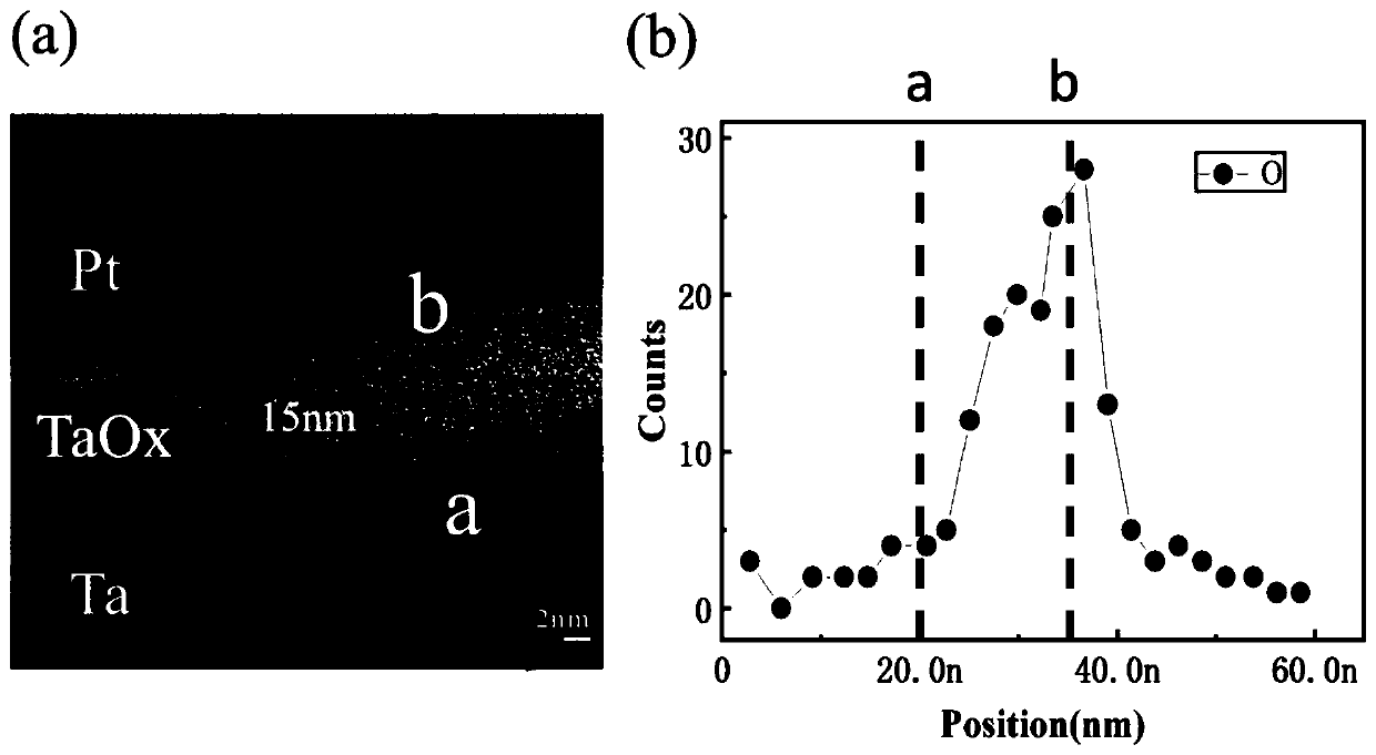
[0073] The functional layer is made of TaOx material, and the TaOx material with oxygen concentration gradient is obtained by contro...
PUM
| Property | Measurement | Unit |
|---|---|---|
| thickness | aaaaa | aaaaa |
| thickness | aaaaa | aaaaa |
| thickness | aaaaa | aaaaa |
Abstract
Description
Claims
Application Information
 - Generate Ideas
- Intellectual Property
- Life Sciences
- Materials
- Tech Scout
- Unparalleled Data Quality
- Higher Quality Content
- 60% Fewer Hallucinations
Browse by: Latest US Patents, China's latest patents, Technical Efficacy Thesaurus, Application Domain, Technology Topic, Popular Technical Reports.
© 2025 PatSnap. All rights reserved.Legal|Privacy policy|Modern Slavery Act Transparency Statement|Sitemap|About US| Contact US: help@patsnap.com


