A kind of Zn in-situ doped p-type hexagonal boron nitride thin film and preparation method thereof
A technology of hexagonal boron nitride and in-situ doping, which is applied in metal material coating process, vacuum evaporation plating, coating, etc., can solve the problem of high toxicity of compounds, and achieve simple method, small impurity ionization energy, low cost effect
- Summary
- Abstract
- Description
- Claims
- Application Information
AI Technical Summary
Problems solved by technology
Method used
Image

Examples
Embodiment 1
[0016] Place the double-sided polished silicon wafer into NH at a volume ratio of 1:1:5 3 ·H 2 O: H 2 o 2 :H 2 O solution, heated in a water bath for 10 minutes; then, the above-mentioned silicon wafer was placed in HCl:H with a volume ratio of 1:1:6. 2 o 2 :H 2 O solution, heated in a water bath for 10 minutes. The main purpose of these two steps is to remove metal ions and organic matter contaminated on the surface of the silicon wafer. Then, the silicon wafer was cleaned for 45 seconds with an HF solution having a volume concentration of 2%, so as to remove the natural oxide layer on the surface of the silicon wafer. Finally, after rinsing the wafer with deionized water, dry it with nitrogen gas for later use.
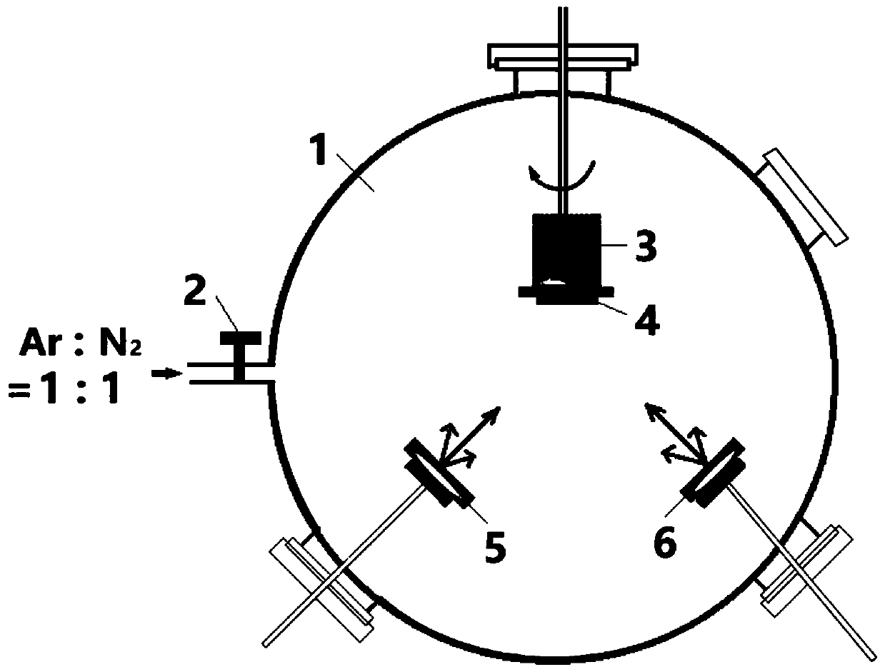
[0017] The hBN target 5 with a purity of 99.95%, the high-purity Zn target 6 with a purity of 99.9995% and the cleaned silicon wafer substrate 4 are placed on figure 1 In the growth chamber 1 shown, the vacuum of the system was pumped to 5×10 -4 Pa, adjust...
Embodiment 2
[0022] The quartz plate was ultrasonically cleaned with acetone for 10 minutes; then, ultrasonically cleaned with absolute ethanol for 10 minutes; finally, ultrasonically cleaned with deionized water for 10 minutes.
[0023] Place the hBN target 5 with a purity of 99.95%, the high-purity Zn target 6 with a purity of 99.9995% and the cleaned quartz substrate 4 on figure 1 In the growth chamber 1 shown, the vacuum of the system was pumped to 5×10 -4 Pa, adjust the target distance of the hBN target 5 to 5 cm, adjust the target distance of the Zn target 6 to 6 cm, turn on the switch of the heating table 3, heat the quartz substrate 4 to 450 ° C, and then open the inlet valve 2 to allow the flow N ratio 1:1 2 Mixed gas with Ar gas, a total of 100 sccm, after the gas flow is stable, adjust the air pressure in the growth chamber to 1.0Pa, and cover the substrate with a baffle; first turn on the RF power connected to the hBN target 5, adjust the voltage to 1600V, and rotate the coupl...
Embodiment 3
[0025] The double-sided polished sapphire slices were ultrasonically cleaned with acetone for 10 minutes; then, ultrasonically cleaned with absolute ethanol for 10 minutes; finally, ultrasonically cleaned with deionized water for 10 minutes.
[0026] The hBN target 5 with a purity of 99.95%, the high-purity Zn target 6 with a purity of 99.9995% and the cleaned sapphire substrate 4 are placed on figure 1 In the growth chamber 1 shown, the vacuum of the system was pumped to 5×10 -4 Pa, adjust the distance between the hBN target 5 and the Zn target 6 to 5 cm, turn on the switch of the heating table 3, heat the sapphire substrate 4 to 500 ° C, and then open the air inlet valve 2 to pass in the gas with a flow ratio of 1:1. N 2 Mixed gas with Ar gas, a total of 100 sccm, after the gas flow is stable, adjust the air pressure in the growth chamber to 1.0Pa, and cover the substrate with a baffle; first turn on the RF power connected to the hBN target 5, adjust the voltage to 1700V, a...
PUM
| Property | Measurement | Unit |
|---|---|---|
| thickness | aaaaa | aaaaa |
| thickness | aaaaa | aaaaa |
| thickness | aaaaa | aaaaa |
Abstract
Description
Claims
Application Information
 - R&D
- Intellectual Property
- Life Sciences
- Materials
- Tech Scout
- Unparalleled Data Quality
- Higher Quality Content
- 60% Fewer Hallucinations
Browse by: Latest US Patents, China's latest patents, Technical Efficacy Thesaurus, Application Domain, Technology Topic, Popular Technical Reports.
© 2025 PatSnap. All rights reserved.Legal|Privacy policy|Modern Slavery Act Transparency Statement|Sitemap|About US| Contact US: help@patsnap.com